n-Type SiC Substrates
Wolfspeed is transitioning to a new wafer scribe format based upon SEMI specification M12-0706. This conversion is projected to be fully integrated across all products by the end of 2023, and brings several improvements. The M12-based scribe will be positioned upright when the major flat or notch is oriented up, making the scribe easier to read when the wafers are loaded into cassettes. The new format includes a wafer supplier identification code, validating the wafer’s authenticity. It also includes a checksum, which is an error-detection method that prevents OCR mis-read errors and reduces the instance of processing errors associated with such event.
Keeping Pace with the World's Demand for SiC Power
Industry-Leading Flexibility and Scale
With more than 30 years of SiC development and manufacturing experience, Wolfspeed produces the industry’s broadest range of SiC materials. Offering n-type conductive SiC products and a variety of SiC epitaxy options, Wolfspeed delivers the quality and quantity necessary to support the rapidly expanding demand for high-efficiency, SiC power semiconductors.
When you partner with Wolfspeed, you get the best and most innovative materials.
Materials Portfolio
- 4H
- 4° Off-axis
- 150 mm
- n-type
- p-type
- Thick epitaxy
n-Type SiC Substrate Product Descriptions
The Materials Business Unit produces a wide assortment of n-type conductive SiC products ranging in wafer diameters up to 150mm. Wolfspeed's industry-leading, high-volume platform process provides our customers with the highest degree of material quality, supply assurance and economies of scale.
Part Number | Description |
|---|---|
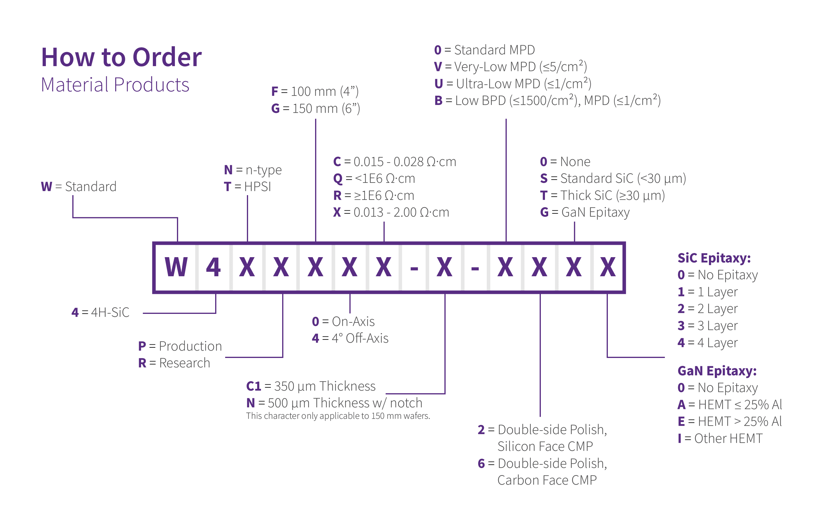
W4NRG4C-C1-V200 | 4H-SiC, n-type, Research Grade, 150mm, 4° Off-Axis, 0.015-0.028 Ω-cm, Very Low MPD ≤5/cm2, 350um Thick w/ 47.5mm Flat, Double-Sided Polish Si Face CMP Epi Ready, Bare Substrate |
W4NPG4C-C1-V200 | 4H-SiC, n-type, Production Grade, 150mm, 4° Off-Axis, 0.015-0.028 Ω-cm, Very Low MPD ≤5/cm2, 350um Thick w/ 47.5mm Flat, Double-Sided Polish Si Face CMP Epi Ready, Bare Substrate |
W4NRG4C-C1-U200 | 4H-SiC, n-type, Research Grade, 150mm, 4° Off-Axis, 0.015-0.028 Ω-cm, Ultra Low MPD ≤1/cm2, 350um Thick w/ 47.5mm Flat, Double-Sided Polish Si Face CMP Epi Ready, Bare Substrate |
W4NPG4C-C1-U200 | 4H-SiC, n-type, Production Grade, 150mm, 4° Off-Axis, 0.015-0.028 Ω-cm, Ultra Low MPD ≤1/cm2, 350um Thick w/ 47.5mm Flat, Double-Sided Polish Si Face CMP Epi Ready, Bare Substrate |
W4NPG4C-C1-B200 | 4H-SiC, n-type, Production Grade, 150mm, 4° Off-Axis, 0.015-0.028 Ω-cm, Ultra Low MPD ≤1/cm2, Low BPD ≤1500/cm2, 350um Thick w/ 47.5mm Flat, Double-Sided Polish Si Face CMP Epi Ready, Bare Substrate |
*C-faced polished wafers and 150mm LBPD substrates available upon request, lead times dependent on volume and requirements
Dimensional Properties, Terminology and Measurements
Flat Length | Linear dimension of the flat measured with automated optical micrometer. |
Primary Flat | The flat of the longest length on the wafer, oriented such that the chord is parallel with a specified low-index crystal plane. |
Primary Flat Orientation | The primary flat is the (1100) plane with the flat face parallel to the [1120] direction. |
Secondary Flat | Not applicable to 150 mm wafers. |
Marking | For silicon face polished material, the carbon face of each individual wafer is laser-marked with OCR-compatible font, similar to the definitions and characteristics in SEMI M12. The laser markings are offset right when looking at the carbon face with the primary flat oriented down. For carbon face polish material, the silicon face of each individual wafer is laser-marked. |
