Jumpstarting a Silicon Carbide based design with the SpeedFit 2.0 Design Simulator
Article
Understanding the in-circuit behavior of Silicon Carbide (SiC) MOSFETs and Schottky diodes in power supplies is a critical component in the design process. As a relatively new technology when compared with silicon-based counterparts, visualizing the performance of these Silicon Carbide components can help a designer more readily leverage this technology.
The SpeedFit 2.0 Design Simulator, based on the commonly-used PLECS simulation platform, offers a comprehensive performance overview based on custom, user-specified data starting with the desired converter topology. After inputting various system parameters, the user is able to virtually test and compare component and topology configurations, switching and conduction loss estimates, and thermal management schemes in their Silicon Carbide based solutions.
The result is a straightforward methodology to leveraging SiC-based power transistors quickly and effectively.
Designing with Silicon Carbide over the PLECS platform
The PLECS platform, developed by Plexim, is a commonly used, web-based simulator (WBS) that is either “standalone” or integrated in Simulink. The standard C scripting interface allows for straightforward modeling and simulation of dynamic systems either as equations, block diagrams, or physical models in the electrical, magnetic (inductors and transformers), mechanical, and thermal domains.
The simulation occurs through an ordinary differential equation (ODE) solver and lumped element models in each respective domain. Analysis tools include steady-state, AC, impulse response, and multi-tone analysis offering accurate models for power converters. Due to the relatively new implementation of SiC when compared with Si power technology, accurate electrical and thermal models that include parasitics (e.g., stray inductance, package inductance) can involve some additional design steps and considerations in most common simulation platforms (LTSpice, PLECS, etc).1
This brings us to an important point, as parasitics, among other factors, lead to a general uncertainty around Silicon Carbide electronics that can potentially delay or otherwise hinder the progress the technology can make in a wide variety of power applications. However, the unique physical properties of Silicon Carbide as the base semiconductor material allows for excellent high-power performance at high switching speeds and voltage levels which, in turn, leads to more efficient, high-voltage, high-power-density converters. This opens up doors for applications with reduced size, weight, and power requirements such as solar micro-inverters, solid-state lighting, converters for clean, large power systems, and even efficient power modules for electric vehicles (EVs).
The process of driving these transistors to minimize conduction and switching losses can be a challenge if a designer has not worked with this technology. Initiating a design with a SiC-based power converter can be accomplished with SpeedFit 2.0 in a seamless web interface to rapidly calculate losses and junction temperature for power devices. It can also help determine the best choice of components for an application, as well as the comparative performance between said components and how this performance varies with different system-level parameters, such as the choice of gate resistance (Rg) for the Silicon Carbide MOSFET.
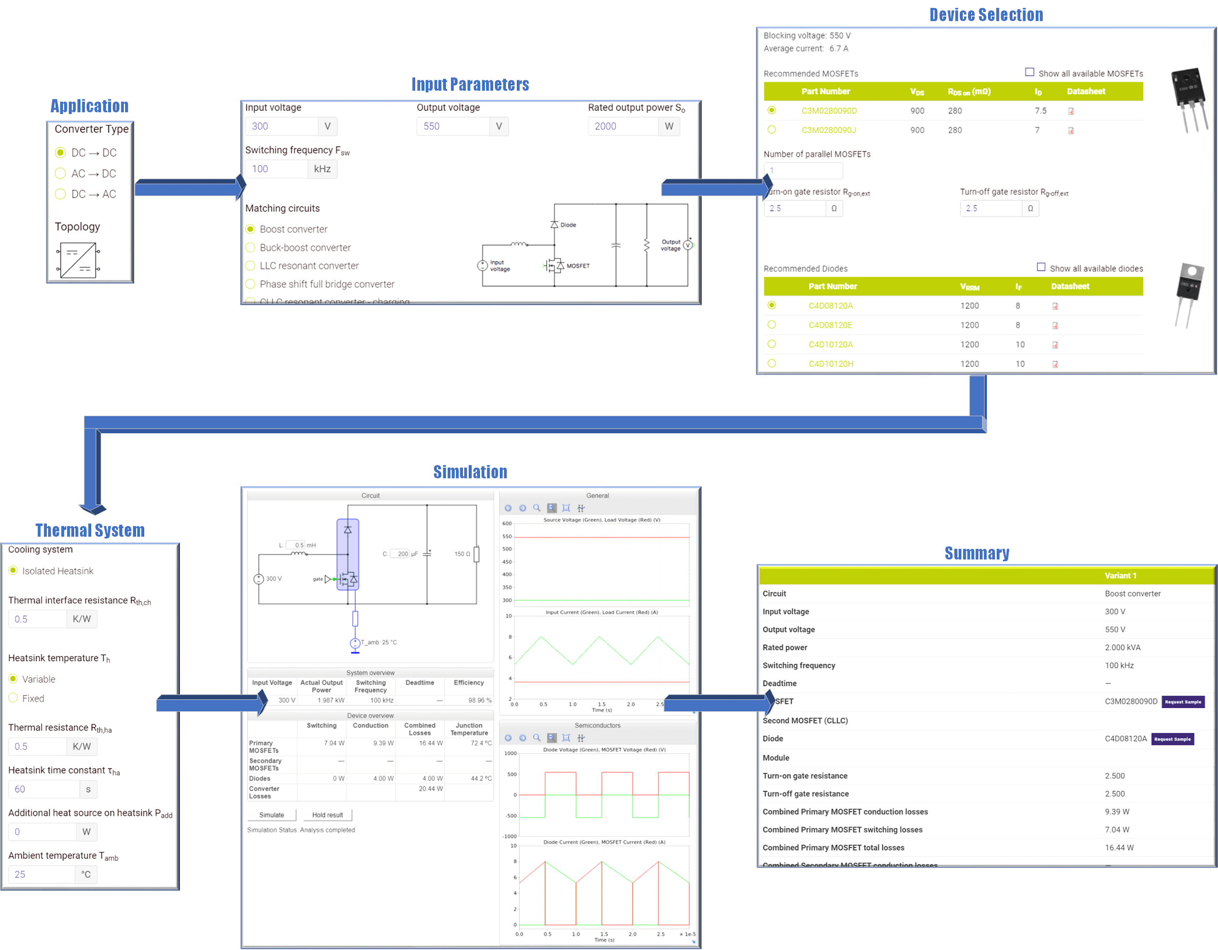
In the case of MOSFETs in particular, the number of devices that need to be paralleled for optimal converter functionality can be ascertained. Instead of spending hours combing through datasheets and making calculations, a designer equipped with basic initial design parameters and waveforms can be empowered to implement Silicon Carbide technology. (Figure 1) lists the step-by-step process an engineer is guided through to start a SiC design using SpeedFit 2.0.

The design process can next be continued through files containing loss and thermal impedance information for Wolfspeed Silicon Carbide devices that are readily available on the Wolfspeed website. This way, PLECS platform users can download and access these models in order to begin the design, fabrication, and testing process with lab results that match simulations.
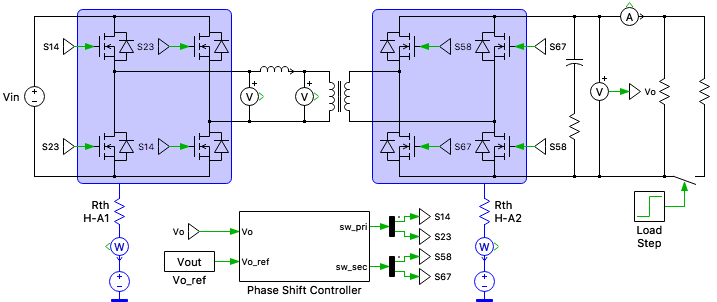
The PLECS standalone tool also includes a free demo mode that offers an array of pre-built SiC designs and can be accessed through Plexim’s website. This affords design engineers a bird’s-eye view of various Silicon Carbide converter/inverter, charging, and power supply topologies and their respective performance. For instance, (Figure 2) shows a sample dual active bridge (DAB) converter featured in PLECS demo model using the Wolfspeed C3M0030090K and C3M0065090D SiC MOSFETs.

Using SpeedFit 2.0 to initiate a Silicon Carbide based design
Entering user parameters
Kicking off a SiC design with SpeedFit 2.0 is simple and straightforward, with a first choice of a general converter type: DC/DC, AC/DC, or DC/AC. The designer is then directed to choose the converter matching circuit within the “Input” tab.
(Table 1) lists the converter type and subsequent matching circuits to choose from.
Converter Type and Matching Circuit Topologies | |
|---|---|
Converter Type | Matching Circuit |
DC-to-DC | Buck Boost Buck-Boost 3-Level Boost Bi-Directional CLLC Phase Shift Full Bridge LLC Resonant Converter |
AC-to-DC | One Phase 2-Level AFE One Phase 3-Level NPC AFE Three Phase 2-Level AFE Three Phase 3-Level NPC AFE Three Phase 3-Level T-Type AFE Three Phase Vienna Rectifier Totempole Converter Bridgeless PRF Boost Rectifier |
DC-to-AC | One Phase 2-Level Inverter One Phase 3-Level NPC Inverter Three Phase 2-Level Inverter Three Phase 3-Level NPC Inverter Three Phase 3-Level T-Type Inverter |
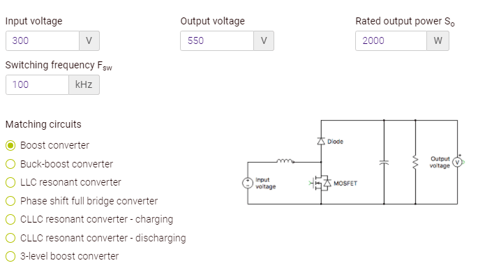
As shown in (Figure 3), the designer is prompted to type input parameters for the chosen circuit, where there is a predefined lower and upper limit for each.2 Passive component values such as capacitance and inductance can be inputted manually or automatically chosen based upon recommended calculations done within the interface.
The list of input parameters for all converter types are as follows:
- Input voltage (VDC)
- Output voltage (VDC)
- Rated output power (W)
- Switching frequency (kHz)
- Switching frequency (kHz) and dead time (ns)
- AC frequency (Hz)
- Power factor

Selecting Silicon Carbide components
After inputting user data, device selection is possible with a list of recommended, commercially available Wolfspeed Silicon Carbide components (e.g., MOSFETs, diodes, modules) and their respective datasheets based upon the input data (e.g., blocking voltage, average current, RMS current). This is helpful for a designer new to working with Silicon Carbide components, as it bypasses the initial navigation through the library of potential components, thereby lowering barriers for implementing SiC-based circuitry. However, the full list of components is still readily available by checking the prompt to “Show all available” components. The selection of components leads to a prompt requesting the number of parallel components for the design, as well as the turn-on/turn-off gate resistance.
Defining thermal system
Following this step, the user is led to define the cooling system and thermal properties of their selected system. It is assumed that the cooling system includes all devices mounted to a common heatsink, with the option of coupling an additional heat source (e.g., auxiliary converter) to the common heatsink. The user defines parameters such as thermal interface resistance. The thermal simulation itself can either be of a variable heatsink temperature — wherein the user defines parameters of thermal resistance, heatsink time constant, any additional power sources on the heatsink, and ambient temperature — or a fixed temperature with a pre-specified value.
Simulation
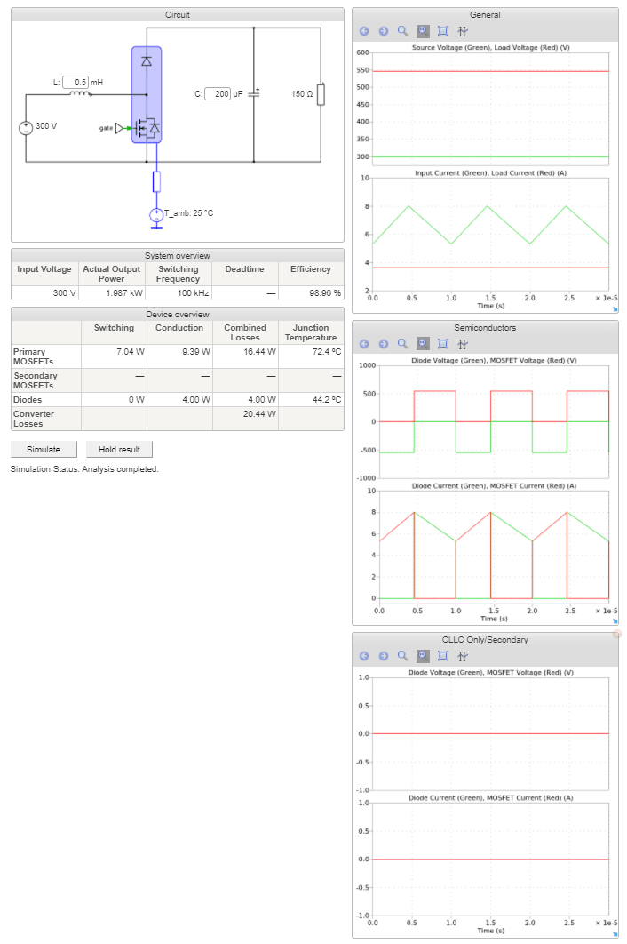
The simulation tab reveals the final circuit model with its respective heatsink configuration and key parameters that have already been specified by the user. A steady-state simulation is performed with several cycles of input/output voltages and current waveforms. As shown in Figure 4, input voltage, rated output power, switching frequency, and efficiency for the system is displayed in the “system overview” table. The “device overview” table displays the total switching, conduction, combined losses, total converter losses, and junction temperature for all MOSFETS, diodes, and modules.

Comparing/changing simulation results
Simulated waveforms can be compared, changed, and adjusted via a results history list that tracks each simulation trace. This way, system parameters such as initial input parameters, components, and thermal parameters can be modified and readily analyzed to offer a seamless basic overview of an initial design iteration.
Designing with SiC over the PLECS platform
SpeedFit 2.0 is a powerful web-based tool for the selection and comparison of Wolfspeed’s Silicon Carbide semiconductor devices in common circuit topologies. The user is able to input realistic system parameters related to their application of interest and virtually test components to estimate losses and expected temperature of the devices in a given application. All of this is accomplished over the widely used PLECS simulation tool to allow design engineers the ability to implement their SiC design over a familiar platform. After choosing the optimal Wolfspeed components, engineers are able to access their device’s loss models and thermal impedance information for offline use in PLECS ― further speeding up the design process.