How Wolfspeed Silicon Carbide Enables Offline Switching-Mode Power Supplies
Article
Silicon Carbide (SiC) technology has improved several systems and subsystem components across a variety of applications. When compared with silicon, Silicon Carbide has demonstrated better power density, and efficiency through faster switching, flat RDS(on) over temperature and at better body diode performance.
This article will explore how Wolfspeed’s SiC components enable offline SMPS systems to excel in terms of efficiency, power density, and overall system cost, particularly when compared with Si and GaN devices.
SMPS trends and comparison between Si, Silicon Carbide, and GaN
Offline SMPS are typically ACDC power systems such as data centers, telecom base stations, and power-mining systems. Data centers consume about 10% of all generated electricity, and if implementing SiC saves even just 1% of energy, that translates into three nuclear power plants (each operating at 1 GW).
When compared with the industry’s standard Generation 1 data center power architecture, Generation 2 removed the uninterruptible power supply and power distribution unit from the AC input, changed the DC bus from 12 V to 48 V, and added a battery backup system to the DC bus (48 V). Because of these changes, the overall system efficiency increased to 85%, saving an energy amount equivalent to 27 nuclear power plants.
The typical specifications for a Generation 2 data center containing an OCP3.0 or HE telecom rectifier are as follows:
- Input voltage range: 180-305 VAC
- Output power: 3,000 W
- Output voltage: 48 V
- Efficiency: 97.5% peak, 96.5% for 30% to 100% load
- Holdup time: 20 ms
- Operating temperature range: 0˚C to 55˚C
The efficiency will vary based on the load percentage, but in general, more than 99% efficiency is required for power-factor correction (PFC) and more than 98.5% efficiency is required for DC/DC converter systems. To meet these new requirements of high efficiency and power density, power designers must look closely at topologies and power components. This can be done with a comparison of technologies including Si, SiC, and GaN-on-Si.
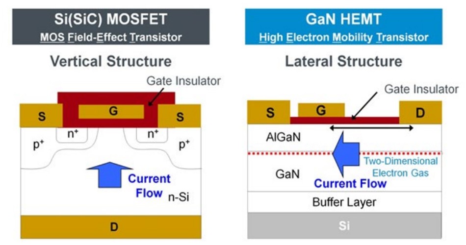
When comparing the physical differences between Si or SiC MOSFETs and GaN high-electron-mobility transistors (HEMTs), it can be observed in Figure 1 that the lateral structure of the GaN HEMT requires an increase in its footprint to accommodate higher power and a different form of current flow, while silicon’s structure is vertical. As an analogy, this is like comparing a vertical “hose” pushing current upward with a “rain gutter” flowing current horizontally.
Additionally, GaN HEMTs cannot avalanche during overvoltage conditions, which can cause catastrophic failures. They also have very poor short-circuit capabilities (a few hundred nanoseconds) and their lattice thermal expansion coefficient mismatches can cause defects.

When analyzing how RDS(on) behaves with respect to temperature, it is seen that SiC outperforms other technologies. Also, most datasheets advertise RDS(on) at room temperature (25˚C), but designers must plan for real junction temperatures that may vary between 120˚C and 140˚C. And it’s important to note that RDS(on) correlates to I2R loss (a conduction loss), which means that the SiC’s 60-mΩ rating is equivalent to 40 mΩ for Si and GaN.
For a more quantified look at how SiC compares with Si and GaN-on-Si, Figure 2 demonstrates how the temperature properties, voltage, and size/package improve when incorporating SiC components.
Parameter | SiC | GaN on Si | Silicon |
|---|---|---|---|
RDS(on) vs Temperature | ~1.4× | ~2.6× | >2× |
Thermal conductivity | 3× | 1× | 1× |
Voltage range | 600V - 10,000V | 40V - 600V | 5V - 10,000V |
Temperature rating | 175°C and above | 150°C | 150°C |
Die Size | 1× | 2× - 3× | 2× - 4× |
Cost | 1× | 1.3× - 2× | 0.5 - 0.75× |
Field hours | >7 trillion | ~20 million | Too many to compute |
Packaging | Standard | Custom | Everything |
Integration | Power Device Only | Gate driver, protection | Simple thru to high |
Figure 2: Technology Capability Comparison Between Si, SiC, And GaN-On-Si
Several other parameters can be compared between the technologies, such as Vgs, junction temperature Tj, RDS(on), capacitance, and recovery during switch. Though SiC doesn’t win out in every category, it does shine in most. With regard to temperature, SiC has the highest Tj,max, which results in a better overall robustness but doesn’t quite have the lowest thermal junction resistance (Rth). However, SiC’s RDS(on) over most operating temperatures is the lowest, which translates to lower loss and higher efficiencies, allowing for maximum power delivery. Because GaN has no avalanche capabilities, SiC’s single-pulse avalanche energy gives it better robustness and protection. What’s more, a higher Vgs,th increases noise immunity and is easier to drive. With respect to switching performance, GaN can provide the lowest Qrr and capacitance, but SiC closely follows. This is important, as it relates to switching losses and efficiency. In general, Si is easy to drive but cannot quite compete with switching performance and losses. GaN shines with regards to switching performance but lacks in robust, and SiC provides an all-around robust efficiency solution with great thermal properties and minimum losses.
Figure 3 shows a direct comparison between IPW60R055CFD7 (Si), C3M0060065J (SiC), and IGT60R070D1 (GaN).
Part Number | VGS(th) min(V) | TJ_max (degC) | RDS(on) (mΩ typical) 25°C | RDS(on) (mΩ typical) 75°C | RDS(on) (mΩ typical) 125°C | Coss tr (pF) | Coss er (pF) | Qrr (nC) | Rth (k/w) |
|---|---|---|---|---|---|---|---|---|---|
IPW60R055CFD7 | 3.5 | 150 | 46 | 64.4 | 88.8 | 1172 | 114 | 770 | 0.7 |
C3M0060065J | 1.8 | 175 | 60 | 63.0 | 70.0 | 132 | 95 | 62 | 1.1 |
IGT60R070D1 | 0.9 | 150 | 55 | 80.0 | 108.0 | 102 | 80 | 0* | 1 |
Figure 3: Key Parameter Comparison Between Si, SiC, and GaN
PFC topology and component selection
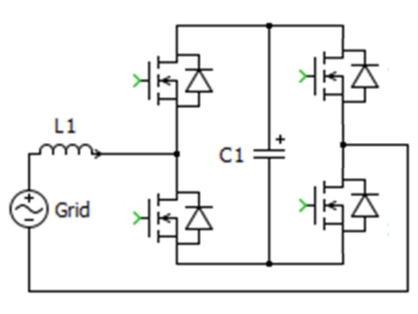
Traditionally, PFC technology requires a bridge rectifier with an LC component, which results in a simple configuration but is bulky and heavy. Today’s industry utilizes an active boost PFC topology, which includes a rectifier and boost component. This configuration is popular to implement and provides adequate performance at a decent cost but is challenged to achieve the latest efficiency standards. The industry is currently evolving to use a bridgeless totem-pole PFC design (shown in Figure 4) that lowers loss and increases power density. This is where SiC MOSFETs can greatly increase efficiency and meet the needs of tomorrow’s designers.

There are several bridgeless PFC solutions to consider for a design, including MOSFET technologies that span Si, SiC, and GaN. When analyzing the component counts/cost, power density, peak efficiency, and gate control requirements, a continuous conduction mode (CCM) totem-pole PFC design utilizing SiC MOSFETs is the clear choice for high-efficiency, high-power–density applications. Figure 5 demonstrates a detailed comparison of a variety of topologies and technologies, highlighting the clear advantages of SiC-based CCM totem-pole arrangements.
#PFC Choke | #Power Semi-conductor | Power density | Peak Efficiency | Cost | Control | Gate Drive | |
|---|---|---|---|---|---|---|---|
Si Conventional CCM PFC | 1 | 3+ | Medium | 98.3% | Low | 1 | 1 |
Si Active Bridge CCM PFC | 1 | 6 | Medium | 98.9% | Highest | 2 | 2 |
Si Dual Boost Bridgeless PFC | 2 | 6 | Lower | 98.6% | Medium | 1 | 1 |
Si Dual Boost Bridgeless PFC SR | 2 | 6 | Lower | 98.9% | High | 3 | 1 |
Si H Bridge PFC | 1 | 6 | High | 98.6% | Medium | 2 | 2 |
Si CrM Totem Pole Bridgeless PFC | 2 | 6 | Medium | 98.9% | Highest | 4 | 3 |
SiC CCM Totem Pole Semi-BL PFC | 1 | 4 | Highest | 98.8% | Medium | 2 | 2 |
SiC CCM Totem Pole bridgeless PFC | 1 | 4 | Highest | 99.1% | High | 3 | 3 |
GaN CCM Totem Pole Semi-BL PFC | 1 | 4 | Highest | 98.8% | High | 2 | 3 |
GaN CCM Totem Pole bridgeless PFC | 1 | 4 | Highest | 99.2% | Highest | 3 | 4 |
GaN CRM Totem Pole bridgeless PFC | 2 | 6 | Medium | 99.1% | Highest | 4 | 5 |
Figure 5: Comparison of Bridgeless PFC Solutions and Technologies
When comparing the same key parameters as before, GaN still has the best switching performance but with a much higher RDS(on) over temperature, which compromises its power-delivery capabilities. And with a very low Vth, it becomes hard to drive and prone to noise. For efficiency, SiC-based CCM totem-pole PFC configurations can have higher efficiencies than Si-based H-bridge topologies and similar efficiencies to GaN. But ultimately its increased reliability and operating temperatures, along with its avalanche capabilities, make it the more robust, reliable choice for a totem-pole PFC design.
Although cost for Si solutions is the lowest, it’s cheaper to implement SiC over GaN for a totem-pole configuration, which puts premium performance at a reasonable price point. A cost analysis was performed for the Wolfspeed SiC C3M0060065J against five equivalent GaN components for a 3-kW totem-pole PFC, and it was found that when comparing power switches, bias supplies, gate drivers and isolation, current sensing, PFC chokes, and cooling costs (heatsinks), some of the GaN devices can cost as much as 84% more than SiC.
CRD-02AD065N is a Wolfspeed 2.2-kW totem-pole PFC module that uses C3M MOSFETs and achieves 80plus Titanium standards (98.8% peak efficiency) while also keeping total harmonic distortion less than 5% under full-load conditions. Design files and related training materials are available on Wolfspeed’s website.
Component and topology selection for DC/DC conversion
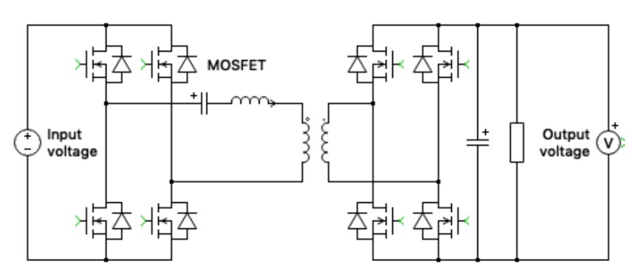
Another approach that can achieve the high efficiencies needed for 80plus Titanium is an LLC resonant converter (shown in Figure 6). This configuration generally provides zero-voltage turn-on, low-current turn-off (which results in low switching losses), high-frequency switching, low-voltage overshoot (making it EMI-friendly), and flexibility for control. This makes the LLC comparable in terms of efficiency and power density.

A key parameter comparison will show similar results as seen in the PFC configuration. SiC has similar switching performance to GaN with better RDS(on) over the full range of temperatures, a higher junction temperature rating, and avalanche capabilities, making it the more reliable choice for power devices used in the LLC.
The CRD06600DD065N is an example of a 500-kHz LLC converter design by Wolfspeed and outputs 400 VDC (closed-loop) or 390–440 VDC (open-loop) at 6.6 kW max with greater than 98% peak efficiency. The related schematic/PCB files are available on Wolfspeed’s website to help kick off and guide a designer through this topology.
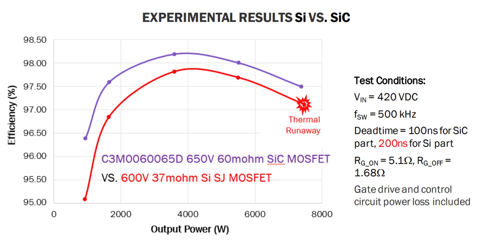
So, for LLC converters, SiC delivers similar power to Si but in a much smaller, lighter form factor due to the integrated and smaller magnetics by enabling higher switching frequency (see Figure 7 for comparison). Experimental results show that when running a Si and SiC MOSFET side by side, the SiC part (C3M0060065 by Wolfspeed) has a higher efficiency due to the flat RDS(on) over temperature, fast switching, and low gate drive power loss. At heavier loads, the Si part enters thermal runaway because of high conduction losses and slower switching.

And when running similar tests with SiC versus GaN, it’s shown that they both have comparable efficiencies at the primary side of the LLC converter.
Final summary
To conclude, 80plus Titanium for offline SMPS systems requires very high efficiency, which SiC delivers with an added robustness factor, enabling high-reliability applications. SiC can provide more than 99% efficiency with obvious advantages for RDS(on) over temperature, a higher junction temperature rating, avalanche capabilities, and with an industry-standard footprint, making it the most suitable choice for power devices used in totem-pole PFC and LLC converter applications.
SiC has become an established technology that is transforming the power industry across many applications, and being that Wolfspeed invented the SiC MOSFET, we’ve seen 7 trillion-plus field hours of Wolfspeed SiC power and a complete portfolio of SiC components/modules that continue to lead the market.