Designed to Last, Even in the Harshest Environments


Article
A ground-up strategy to enable better system durability in tough operating conditions
Introduction
Reliability is the consistency of a measure or a method. And the importance of reliability to our industry can hardly be overestimated. What is not discussed as much is the necessary step-function to reliability: What we at Wolfspeed call “durability,” or to some, the concept of “ruggedness.” Applications like electrified marine and railway inverters, commercial and heavy-duty vehicles, renewable power plants and pulsed power systems are pushing the operational limits for electric power systems. The ever-increasing demand for system durability in these applications evokes a new set of design challenges and performance expectations. Construction and agriculture OEMs are electrifying. Despite being adjacent to the automotive market, the e-mobility design challenges and operating environment are very different. These systems must contend with some challenging operational conditions. Some of this machinery is active in the upper northern hemisphere for the harvesting season and must survive plummeting temperatures. When spring and summer seasons rolls back around -- and workers return to the field -- they need to trust that their SiC-based inverters are going to “wake up” after spending time in the elements where below -40°C are the norm.
At the same time, the traction drives for heavy-duty and agricultural sectors are subject to much heavier loads for longer durations than drives in the automotive industries. For example, a tractor plowing a field may typically operate at 80% of its rated power continuously over the course of a workday. Construction equipment in mining operations is often operated continuously between scheduled maintenance. While in the field, the speed of a tractor is typically slow (less than 20 km/h), engine power is typically high and continuous, and the ambient temperature can be high. Slow-moving vehicles cannot quickly escape their self-generated heat cloud, and moderate tailwinds can prevent escape from that cloud. These two examples are two extremes of operating conditions for the same application. And this is only the tip of the iceberg: electrified marine systems are subject to high humidity, industrial processing plants require continuous system operation in corrosive environments and every application at high altitude contends with cosmic radiation. The power electronics industry must recognize these increasing end-system performance expectations and proactively address them.
This whitepaper explores how Wolfspeed strategically invests in technology, processes, and people to create silicon carbide products that deliver the next level of ruggedness at every stage of the product life cycle.
Reliability Bathtub Curve
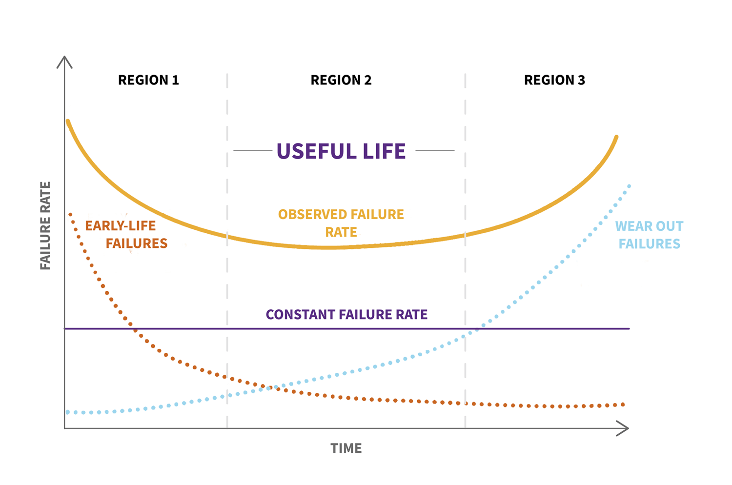
Before delving into durability, let’s first address some reliability fundamentals. Reliability engineers use the bathtub curve model to characterize and predict device failure patterns across operational lifespans (Figure 1). This statistical representation divides device reliability into three distinct regions, each governed by different failure mechanisms and requiring specific mitigation strategies. Understanding these regions is essential for developing robust power semiconductor devices capable of meeting the demanding requirements of modern electrified systems.
Region 1 encompasses early-life failures due to manufacturing defects, material impurities, or process variations that escape initial screening. This phase is critically dependent on comprehensive device qualification protocols, including accelerated stress testing, burn-in procedures, and statistical process control measures that identify and eliminate weak devices before field deployment.
Region 2 represents the operational lifetime characterized by a constant, low failure rate driven by random events such as cosmic radiation-induced single event burn-out, electrical overstress conditions, or environmental factors beyond normal operating parameters. For power semiconductor devices, this region’s failure rate is quantified through extensive field data collection spanning thousands to millions of device-hours, plus advanced testing under high radiation exposure at national laboratory facilities, thus enabling accurate Failure-In-Time (FIT) rate calculations essential for system-level reliability predictions.
Region 3 encompasses end-of-life wear-out mechanisms where cumulative damage from electrical and temperature stress, thermal and power cycling, bond wire fatigue, and other degradation processes leads to increasing failure rates. This phase relies heavily on physics-of-failure models, accelerated aging studies, and Mean Time To Failure (MTTF) calculations to predict device lifetime under specific operating conditions.
Modern SiC power devices face unique reliability challenges compared to traditional silicon technologies. The wide bandgap properties of silicon carbide, while enabling superior high-temperature and high-voltage performance, introduce specific failure mechanisms such as threshold voltage instability, gate oxide reliability concerns, bipolar stability and cosmic ray sensitivity that must be addressed through advanced device design and qualification methodologies.
Minimizing Early Device Failures
Silicon carbide demonstrates superior durability compared to silicon due to its wider bandgap, higher breakdown voltage, exceptional thermal conductivity, and robust crystal structure. These intrinsic properties enable SiC devices to operate at higher temperatures, voltages, and frequencies while maintaining reliability in harsh environments. After years of advanced research in wide-band gap materials, the founders of Wolfspeed felt incredibly convicted to commercialize silicon carbide so high power systems could benefit from SiC’s three times wider band gap and ten times higher dielectric breakdown field. Wolfspeed launched the industry’s first SiC MOSFET in 2011 and has been working hard to lead the transition to SiC ever since.
Today, Wolfspeed is a pure-play silicon carbide device and materials manufacturer. Vertical integration provides Wolfspeed with full control over innovation on materials and device levels enabling greater control over quality, cost and innovation speed. This integrated approach enables precise customization of SiC crystal quality for specific applications, better alignment between the materials and device R&D teams and continuous rapid feedback loops from device manufacturing facility to materials manufacturing facility to optimize processes and maximize product performance.
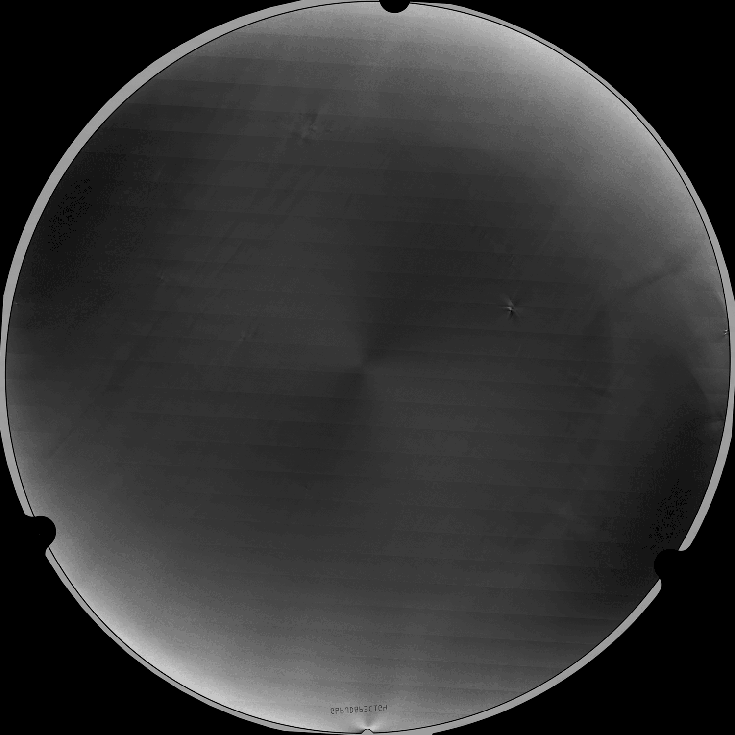
The latest release of 200mm bare wafer and epitaxy is an excellent example of continuity of quality improvements. The improved crystal growth process for 200mm SiC has resulted in 200mm wafers with reduced micropipe densities (MPDs), threading screw dislocations (TSDs), basal plane dislocations (BPDs), and overall etch pit densities (EPDs) compared to our current 150mm SiC wafers. Overall processing improvements from improved 200mm equipment capabilities has already resulted in good wafer shape, lower residual stress, and improved surface parameters. Importantly, the learnings from 200mm are affording continuous improvement for 150mm SiC wafers.
Overall end-to-end control – from crystal growth to finished devices – translates into better performance, faster time-to-market, better control over supply security.
Gate oxide breakdown
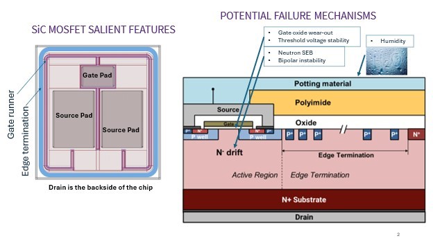
SiC MOSFETs have aggressive reliability requirements: A high blocking voltage requires a high electric field reliability, while a high gate oxide electric field needs a high gate oxide reliability. A high switching frequency necessitates a high threshold voltage (VGS(th)) stability, high body diode is requisite for third-quadrant operation, and finally, there is a need for high terrestrial neutron reliability for high-altitude applications. SiC MOSFETs involve several salient features that, when optimized, offer high quality and reliability.
Stressors of a SiC device include blocking voltage, gate voltage, temperature, humidity, and radiation. Gate oxide wear-out and increased threshold voltage can occur over time in SiC MOSFETs due to the application of a higher electric field relative to Si-based devices. Figure 3 shows the common failure mechanisms in SiC devices. Wolfspeed employs industry-standard as well as novel, custom reliability tests to ensure reliable operation of the MOSFET.
For example, extensive reliability testing and life-time predictions show that Wolfspeed’s MOSFET median gate oxide lifetime is more than 10,000 years at 175oC.
With these common failure mechanisms in mind, Wolfspeed utilizes proven industry-standard testing to ensure the SiC devices are of the utmost quality and reliability prior to releasing them (Table 1). This includes the qualification testing with large sample sizes sampled from different lots, to ensure a low failure rate with high statistical confidence.
Wolfspeed leverages industrial (JEDEC) and automotive standards (AEC-Q101) that were constructed around silicon. The AEC standards demand more stringent device acceptance criteria, including parametric drift; being able to meet those criteria requires aggressive electrical and optical screening. The major industry consortia including JEDEC, IEC, AEC, and JEITA are all actively developing SiC-specific standards to meet the needs for SiC technology and customer base.
Wolfspeed is integrally involved in this process, working with subcommittees and task groups on SiC reliability and qualification testing.
Test | Is it Required? | Lot Size | Test Conditions |
|---|---|---|---|
DPA – Destructive Physical Analysis | Y | 3 Lots; 2 Samples per test (Auto) | Random sample of parts that have successfully completed H3TRB and Thermal Cycling (TC) |
PC – Preconditioning (AEC-Q101 Rev. E): MSL Level 1 | Y | 2 Lots; 11 Samples (I&E) | Electrical test + External Visual Inspection + 24 hr. bake at 125°C + Damp Heat 85°C, 85% RH, 168 hrs. + reflow 3X@245°C + Electrical test only |
PC – Preconditioning (AEC-Q101 Rev. E): MSL Level 3 | Y | 2 Lots; 11 Samples (I&E) | Electrical test + External Visual Inspection + 24 hr. bake at 125°C + Damp Heat 30°C, 60% RH, 192 hrs. + reflow 3X@245°C + Electrical test only |
PV – Parametric Validation | Y | 3 Lots; 25 Samples (Auto) | Static Tests @ Tj = -40°C, 25°C, 175°C (cold, room, hot) |
MSL – Moisture Sensitivity Level | Y | 2 Lots; 11 Samples (I&E) | JEDEC J-STD-020 |
HTRB – High Temperature Reverse Bias | Y | 3 Lots; 25 Samples (I&E) 3 Lots; 77 Samples (Auto) | Vds=80% Vds, Vgs=0 V, Ta=175C, 1000hrs |
HTGB – High Temperature Gate Bias | Y | 3 Lots; 25 Samples (I&E) 3 Lots; 77 Samples (Auto) | Vgs=+Vgsmax, Vds=0 V, Ta=Tmax, 1000hrs Vgs=-Vgsmin, Vds=0 V, Ta=Tmax, 1000hrs |
GSS – Gate Switching Stress | N | 3 Lots; 25 Samples (I&E) 3 Lots; 77 Samples (Auto) | Vgs= -Vgsmin to +Vgsmax, Ta=25°C, 1E12 cycles |
TC – Temperature Cycling | Y | 3 Lots; 25 Samples (I&E) 3 Lots; 77 Samples (Auto) | Ta=-40°C / 150°C, 1000 cycles |
H3TRB – High Humidity High Temp Reverse Bias | Y | 3 Lots; 25 Samples (I&E) 3 Lots; 77 Samples (Auto) | Vds=100 V, Vgs=0 V, 85%RH, Ta=85°C, 1000hrs |
HV-H3TRB – High Humidity High Temp Reverse Bias | N | 3 Lots; 25 Samples (I&E) | Vds=80% Vds, Vgs=0 V, 85%RH, Ta=85°C, 1000hrs |
IOL – Intermittent Operational Life | Y | 3 Lots; 25 Samples (I&E) | ΔTj ≥ 100°C, Ta = 25°C, 1000hrs |
ESD – HBM and CDM | Y | 1 Lot; 18 Samples (I&E) 3 Lots; 10 Samples (Auto) | Per AEC-Q101 |
UHAST – Unbiased HAST | Y (is required for Auto) | 3 Lots; 25 Samples (I&E) 3 Lots; 77 Samples (Auto) | Ta = 130°C, RH = 85%, 96hrs |
Applications such as marine inverters and motor drives need to survive in high humidity, and the standard H3TRB qualification will no longer suffice. It is advised to use the electronic components that pass the more aggressive HV-H3TRB qualification. HV-H3TRB (High Voltage, High Humidity, High Temperature Reverse Bias) testing represents one of the most stringent reliability qualification tests for semiconductor power devices, simultaneously subjecting components to maximum reverse bias voltage, elevated humidity levels (typically 85% RH), and high temperatures (85°C or higher) for extended durations of hundreds to thousands of hours. This accelerated environment stress test simulates the harshest real-world operating conditions in compressed timeframes, validating device robustness under the combined electrical, thermal, and environmental stresses encountered in demanding applications such as automotive powertrains, industrial motor drives, and outdoor power systems. As a critical requirement for high humidity applications, successful HV-H3TRB testing with zero failures and no parameter degradation beyond specified limits demonstrates that semiconductor devices can maintain reliable operation throughout their intended lifespan, even when exposed to the extreme conditions that would typically accelerate failure mechanisms like corrosion, electromigration, and dielectric breakdown. Wolfspeed offers 2 families of power modules in industry-standard footprint qualified for HV-H3TRB: 1200V and 1700V half-bridge modules in 62mm footprint (BM) and 1200V and 2300V Wolfspeed Wolfpack™ available in half-bridge, full-bridge, T-type, and 6-pack configurations.
Maximizing Useful Life
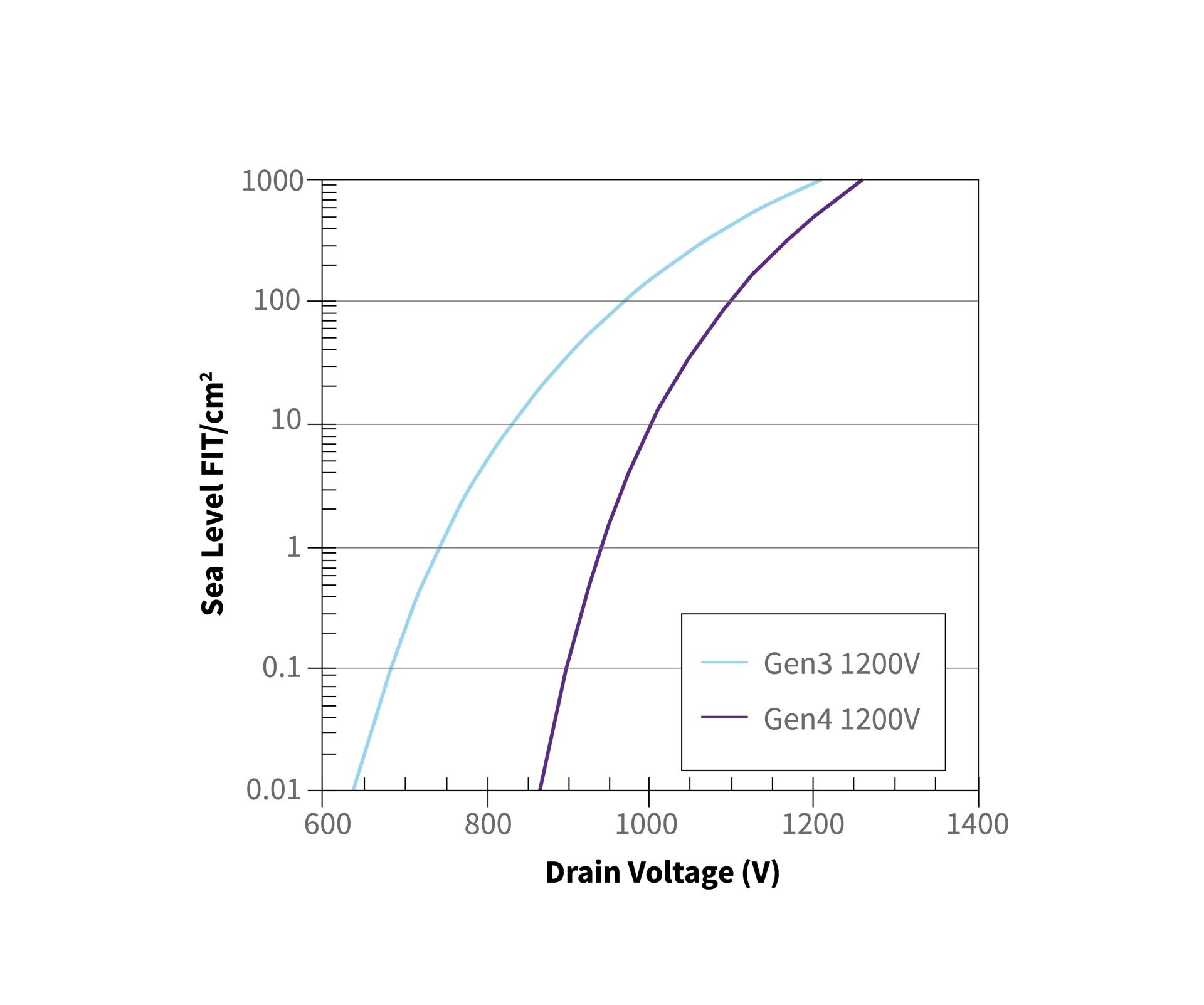
Random failure mechanisms in qualified SiC devices are predominantly attributed to cosmic radiation-induced single event burn-out, particularly relevant for high-altitude applications such as wind farms in mountainous regions or aerospace systems. While SiC devices inherently demonstrate higher cosmic ray immunity than silicon counterparts due to their smaller die size and reduced neutron interaction area, Wolfspeed has deliberately addressed this challenge in its Gen 4 MOSFET technology. The YM4 family represents a significant advancement in power module technology, leveraging Gen 4 MOSFET technology within a 1200V six-pack SiC module configuration (YM platform). Enhanced device structures and optimized gate oxide designs deliver up to 100X improvement in Failure-In-Time (FIT) rate compared to previous generations, effectively mitigating cosmic radiation-induced failures. This substantial enhancement enables system designers to deploy these modules in safety-critical applications such as automotive powertrains, aerospace systems, and industrial equipment operating in high-altitude or space-adjacent environments. This improvement reduces the need for excessive voltage derating, enabling more efficient system designs. Additionally, they can survive overload and overstress events, with Wolfspeed select die portfolio qualified for continuous operation at 185°C and limited life operation at 200°C.
Beyond cosmic ray immunity, the YM4 platform’s Gen 4 MOSFET technology significantly reduces VDS overshoot during switching transitions, addressing a key limitation that has historically constrained system performance. Lower voltage overshoot allows engineers to operate systems closer to the device’s rated voltage limits without compromising reliability or increasing FIT rates, effectively expanding the usable operating envelope. This characteristic enables more aggressive system designs with higher power densities and improved efficiency, as designers can confidently push switching frequencies and power levels without the traditional safety margins required to accommodate voltage spikes. The combination of enhanced cosmic ray immunity and reduced overshoot fundamentally changes the reliability equation for high-performance power conversion systems, allowing OEMs to achieve previously unattainable levels of system performance while maintaining the stringent reliability requirements demanded by mission critical applications.
Short circuit withstand time, a critical parameter for motor drives and traction systems, ensures safe shutdown during faults. The automotive die EM4E120-025D100 based on Gen 4 technology can tolerate up to a two-microsecond (2.3μs) short circuit energy compatible with existing gate driver technologies without compromising RDS(on) performance. This expands the Safe Operating Area (SOA), ensuring robust performance and enables designers to reduce semiconductor usage, lowering costs without compromising safety.
Stable threshold voltage characteristics under high drain-source voltage conditions are critical for maintaining predictable switching behavior and minimizing power losses in SiC power devices. Unlike conventional silicon MOSFETs that exhibit significant threshold voltage drift with increasing drain-source voltage due to Drain-Induced Barrier Lowering (DIBL) effects, our MOSFETs maintain consistent gate control across their entire voltage operating range. This threshold voltage stability ensures that switching timing remains predictable regardless of the applied drain-source voltage, enabling precise control of turn-on and turn-off transitions essential for high-frequency switching applications.
Additionally, the stable threshold voltage prevents unwanted device turn-on during high voltage blocking states, significantly reducing leakage currents that would otherwise contribute to power losses and thermal stress. This characteristic is particularly valuable in applications such as automotive powertrains and renewable energy systems, where devices must reliably block high voltages while maintaining low standby losses and consistent switching performance across varying load conditions and operating voltages.
Mitigating Intrinsic Wear-out Failures
Blocking voltage and gate voltage long-term wear-out
The reliability testing of SiC devices and the various lifetime prediction models reveal the typical failure mechanism as the device ages. Wolfspeed employs common testing techniques for intrinsic wear-out by pushing the device to way over the maximum voltage rating or current rating for as long as possible and under the worst conditions possible. In Figure 5, a 1,200V - rated Wolfspeed MOSFET is pushed up to 1,600V and predicted hours of operation are obtained based upon this stress.
It should be noted that a 1,200V - rated Si device generally rolls off at about 1,250V; therefore, SiC devices generally have much more margin on their voltage ratings. Typically, a 1,200V–rated SiC MOSFET is working on a 700 to 800V bus — in this case, there are over 300 million hours of theoretical safe operation before the device fails from a failure mechanism due to blocking voltage. The very same process is applied to gate voltage with the TDDB method.
The TDDB method is another method of understanding the MTTF of power devices. This method subjects a population of MOSFETs to a constant bias at accelerated bias conditions as well as elevated temperatures. The failure time statistics are calculated and Weibull distributions are fit to the failure statistics to estimate lifetime. In Figure 5, a device with a gate voltage rating of 15V is pushed to beyond 35V and the probability of failure at the rated gate voltage becomes 50 million device hours. For the Gen3 650V Wolfspeed MOSFETs, the MTTF stands at 70 million hours at 15V continuous gate bias, showing a nearly identical gate reliability to the 1,200V and 1,700V MOSFETs.

Power cycling is a standard reliability test used to assess semiconductor packaging under conditions that mimic real-world switching environments. It is particularly critical for SiC (silicon carbide) devices, which operate at higher power densities and elevated temperatures compared to traditional silicon.
Power Cycling and Packaging Reliability
While extensive efforts are being made to ensure successful operation of SiC bare die, the power and thermal cycling capabilities and packaging robustness remain critical determinants of useful application lifetime for both Si and SiC technologies. Typically, power packaging is the weakest link, especially at higher temperatures where the failures tend to be more intrinsic in nature (e.g., wire bonds and die attach rip off). The Gen 4 family of SiC power modules represents a significant advancement in power electronics reliability and thermal management.
Read the whitepaper to learn how Wolfspeed is enhancing system durability with advanced packaging technology.
The YM4 6-pack SiC modules demonstrate exceptional durability, delivering three times more power cycles at operating temperature compared to competing SiC solutions (see Figure 6). This enhanced cycling capability translates to extended operational lifespans and reduced maintenance requirements in demanding industrial applications.
Read the whitepaper to learn about Wolfspeed's approach to power cycling and lifetime modeling.
The TM4 1200V automotive overmolded modules showcase superior thermal engineering through innovative packaging technologies. By implementing copper clip bonding combined with silver-sintered packaging, these modules achieve up to 8% improvement in thermal performance while simultaneously enhancing power cycling capabilities.
The copper clip bond technology eliminates traditional wire bonds, reducing thermal resistance and improving current distribution across the die. This combination of advanced packaging techniques addresses critical automotive requirements for thermal management and long-term reliability.
Wolfspeed’s WolfPACK™ family incorporates Aluminum Nitride (AlN) substrates as a critical thermal management innovation. AlN’s exceptional thermal conductivity properties enable up to 50% Reduction in Thermal resistance (RTH) compared to conventional substrate materials. This significant improvement in heat dissipation directly translates to enhanced power density capabilities and improved reliability under hightemperature operating conditions. The superior thermal performance of AlN substrates, combined with their excellent mechanical robustness, allows Wolfspeed Wolfpack™ modules to maintain optimal junction temperatures while withstanding thermal cycling stresses.
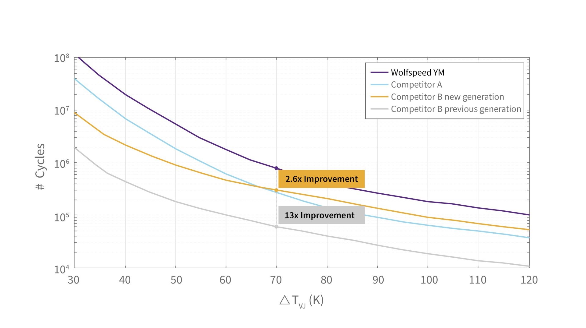
Figure 6: YM4 lifetime reliability analysis
The above techniques, plus the Gen 4 MOSFET technology position SiC modules as the optimal solution for high-performance applications requiring exceptional thermal performance, extended operational life, and robust power cycling capabilities in both industrial and automotive sectors.
Another example of evolving performance expectations came from a leading power supply manufacturer who has encountered significant infrastructure challenges driven by rapid AI deployment and expansion. The accelerated growth in computational requirements has necessitated comprehensive redesign of data center layouts, including strategic relocation of Uninterruptible Power Supply (UPS) systems to accommodate increased server density. This infrastructure optimization has created new environmental considerations, particularly regarding component placement in areas with elevated sulfur concentrations. The potential exposure to sulfuric environments during facility reconfiguration has prompted evaluation of component reliability under these specific conditions. This application scenario demonstrates the importance of environmental qualification testing, ensuring power electronics maintain performance integrity across diverse installation environments within modern data center facilities.
The 1200V Wolfspeed Wolfpack™ family, including modules such as the CAB006A12GM3, has successfully completed rigorous qualification testing for operation in high sulfur environments containing Hydrogen Sulfide (H2S). This certification demonstrates the modules’ ability to withstand corrosive sulfur compounds that can degrade electronic components and compromise system reliability. The robust packaging and materials engineering of the WolfPACK™ family provide exceptional resistance to sulfur-induced corrosion, making these modules ideal for challenging industrial applications including oil and gas processing, geothermal power generation, and chemical manufacturing facilities. This H2S qualification expands deployment opportunities in harsh environments where traditional power electronics would experience accelerated degradation, ensuring reliable longterm operation in sulfur-rich atmospheres.
Wolfspeed’s reliability bathtub curve calculator
In order to generate predictions of the useful life and end-of-life regions of the bathtub curve for SiC devices, Wolfspeed developed a bathtub curve calculator that uses a mission profile as input. The bathtub curve calculator is essentially a prediction of the failure rate of the device as a function of time in the field, due to the failure rate contributions from failure mechanisms such as single-event-burn-out and gate oxide wear-out due to gate or blocking voltage.
Figure 7 shows an example failure rate prediction based on a typical application mission profile input of a tabulation of hours at gate voltage, blocking voltage, temperature and, altitude. With this reliability prediction tool, Wolfspeed can provide customers with valuable information about the expected reliability of SiC devices for their target application conditions.
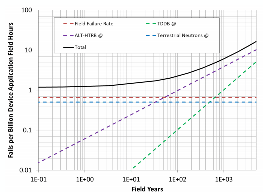
Figure 7: Wolfspeed SiC bathtub curve calculator
Conclusion
The evolution from reliability to ruggedness represents a fundamental shift in Wolfspeed’s technology philosophy, driven by the extreme operational demands of emerging electrified applications. As construction equipment endures Arctic winters, agricultural machinery operates at continuous high power in challenging thermal environments, and marine systems face relentless humidity exposure, traditional reliability metrics alone are insufficient to guarantee system performance.
Wolfspeed’s strategic investment in advanced technology, rigorous qualification processes, and comprehensive ruggedness testing addresses these escalating performance expectations head-on. By developing silicon carbide solutions that withstand temperature extremes from -40°C to 185°C continues and 200°C limited, sustained high-power loading, and harsh environmental conditions, we enable OEMs to confidently electrify their most demanding applications.
The transition to electrified heavy-duty, agricultural, and marine systems is not merely an extension of automotive electrification-it requires a new paradigm of semiconductor ruggedness. Through our end-to-end approach - encompassing materials science, device design, and qualification methodologies - Wolfspeed delivers SiC power devices that don’t just meet specifications but exceed the durability expectations of mission-critical applications where failure is not an option.
As industries continue pushing the boundaries of electrification into increasingly challenging environments, the distinction between reliable and rugged becomes the difference between systems that function and systems that endure. Wolfspeed’s commitment to durability ensures that when operators return to the field after harsh winters or when mining equipment faces continuous operation cycles, their SiC-based power systems are ready to perform - season after season, shift after shift.