Advantages of SiC over Si for Unidirectional On-Board Chargers
Article
On-board chargers (OBCs) for electric vehicles (EVs), such as battery electric vehicles (BEVs) and plug-in hybrid electric vehicles (PHEVs), convert the AC power from the grid into the DC to power the battery within the vehicle. Because these are placed inside the vehicles, the weight, size and efficiency become key design considerations.
Still, range anxiety is an observable phenomenon across EV owners wherein drivers consistently fear being stranded with an EV that has lost charge. In order to offset the negative influences of this, the battery capacity of EVs is being worked upon with an additional increase in charging power levels. Silicon carbide (SiC) components are well suited for these systems due to their high power density and thermal conductivities, allowing them to operate more efficiently with far less components to accomplish the same power levels as silicon (Si)-based OBCs.
This article is part of a two-part series that discusses the design considerations of OBC systems and the advantages that SiC has over Si in such designs. The practical advantages of implementing SiC over Si for OBCs are detailed in a head-to-head comparison of Si and SiC based OBC designs with a cost and system benefit breakdown.
Key design factors for OBCs
Typically, chargers have been off-board or fixed chargers that are not installed inside the vehicles. OBCs allow the vehicle to convert AC input from the grid (e.g., at home, at a charging station, etc.) into DC power to charge the battery bank of the EV. The standard battery size for HEVs range from 3 kWh up to 20 kWh, whereas BEV commuter cars and trucks have higher capacities, from 20 kWh to 300 kWh. The higher the conversion level of the charger, the quicker the battery charges, allowing for repeatable, rapid charges. The standard power levels of OBCs have stemmed from the standard AC mains power level — 120 VAC. OBCs typically range from 1 kW for e-bikes; 3.3 kW for HEVs/PHEVs, typically with a 120-V/30-A input; 6.6 kW for commuter car BEVs, with a 240-V/30-A input; 11 kW for truck BEVs, often with 440-V/15-A three-phase power; all the way to 22 kW for performance and commercial vehicles, with a 440-V/30-A three-phase input. OBCs can either be unidirectional or bidirectional in nature, where a bidirectional charger has the ability to allow power to flow from the input to the output as well as from the output to the input. A bidirectional charger has the additional ability to achieve higher system efficiencies by omitting diode losses, allowing for smart vehicle-to-grid functions (e.g., peak shaving, frequency regulation, etc.), and allows for vehicle-to-home power and acts as a battery bank in the case of a power outage.1
SiC based unidirectional OBCs reduce system complexity with less active circuit components. This allows for lower system cost and more compact OBC size — two critical factors in OBC design. Due to their relative simplicity and lower cost, unidirectional OBCs are anticipated to continue to be popular over the next five to ten year period.
The following are major factors to consider in OBC systems:
- Cost
- Size
- Weight
- Efficiency
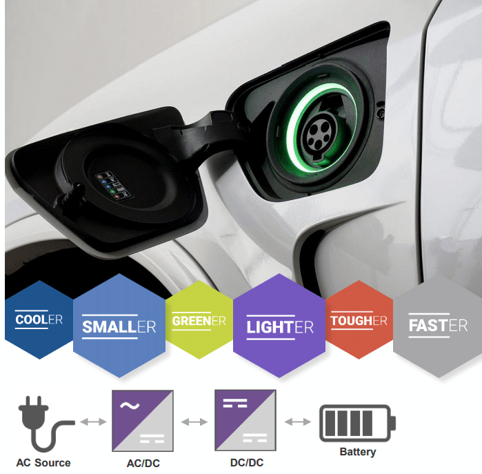
Smaller and lighter EVs demand smaller and lighter OBCs (Figure 1). This also leads to power density and integration considerations wherein the OBC and DC/DC converters are often in one-box configurations, minimizing size and weight. In some cases, OBCs are mounted to an internal inverter that allows the EV to self-charge the battery through regenerative braking from the drivetrain. Moreover, the costs of these systems must help close the price gap with ICE in order to stay competitive. All the while, these higher-powered OBC systems are best used only when they operate efficiently — thus allowing for charging. This is especially true with smaller EVs and motorcycles/scooters that are expected to charge extremely quickly.
Understanding how SiC has inherent advantages over Si for OBCs
With all these considerations in mind, the SiC base material loosens design constraints on OBCs with its inherent advantages. Table 1 lists the semiconductor properties of SiC, compared with the traditionally used Si-based OBC.
Semiconductor Properties of Substances Used in OBCs | |||
|---|---|---|---|
Properties | Si | SiC | GaN |
Band Gap (eV) | 1.12E+00 | 3.3 | 3.44 |
Breakdown Electric Field (V/cm) | 4.00E+05 | 2.00E+06 to 4.00E+06 | 5.00E+06 |
Electron Mobility {cm2/Vs) | 1100 | 370 | 1500 |
Saturation Conductivity | 1.00E+07 | 2.00E+07 | 2.70E+07 |
Thermal Density (W/cm C} | 1.5 | 3.7 | 1.3 |
Power Intensity (W/mm) | .8 | 4 | 7 |
Power Device Figure of Merit | 1 | 675 | 3000 |
Wide-bandgap (WBG) semiconductors are known to allow devices to operate at much higher voltages, frequencies, and temperatures than conventional semiconductors such as Si. This, in combination with SiC’s high critical field breakdown voltage, saturation velocity, electron mobility, power density, and thermal conductivity allows the SiC power device to withstand high power with a simpler thermal management system. These inherent benefits can now be taken advantage of within a budget due to the advancements in SiC fabrication technology — wafer diameters have grown, allowing for more circuits to be processed per batch. Because of these qualities, SiC-based converters and inverters function at faster switching speeds and higher junction temperatures[1] [2] , with the ability to rapidly shift heat away from the die while simultaneously maintaining cost-effectiveness. Figure 2 describes two standard unidirectional charging powers (3.3 kW, 6.6 kW, 11 kW, and 22 kW), as well as key OBC design trends.
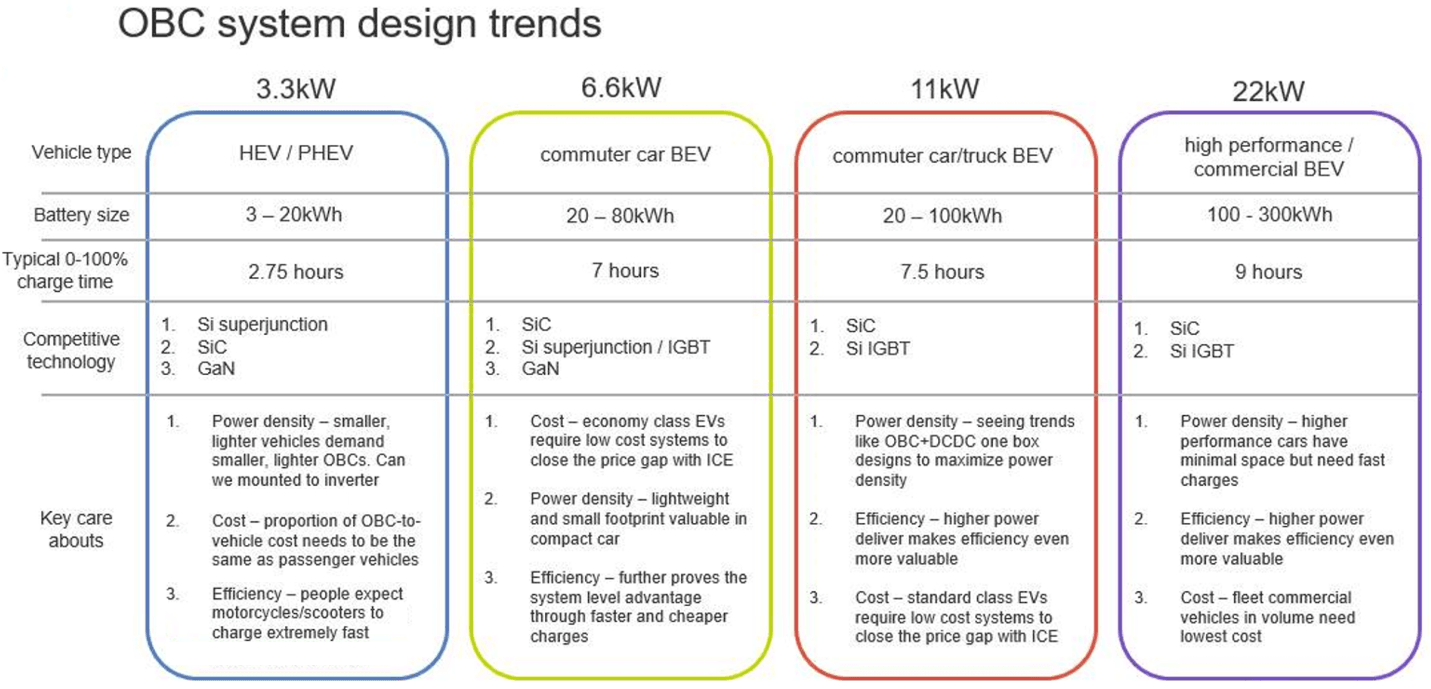
While gallium nitride (GaN) and Si-based superjunction (SJ) technologies compete with SiC for the 3.3-kW and 6.6-kW chargers, Si IGBTs compete with SiC for higher-powered, 11-kW and 22-kW OBCs. As shown in Table 1, similar to SiC, GaN is also a WBG semiconductor with nearly double the power density and a higher electron mobility — allowing it to operate at higher frequencies and with more power per volume. For these reasons, GaN is often used in high-power RF applications. However, the GaN substrate offers only a third of the thermal conductivity the SiC substrate has. In other words, while the power density may be high, the ability of the material to readily dissipate heat is far less than that of SiC, causing it to be less ideal for medium- to high-powered applications. Moreover, the GaN substrate is relatively pricey when compared with SiC. So while GaN-based OBCs can operate some of the highest power densities with a high converter efficiency (with GaN-on-SiC technologies), the thermal limitations, high price point, and the complex control mechanism for GaN transistors can often cause this technology to be a less desirable solution.1
As shown in Figure 2, Si-based power technologies are often utilized due to their cost-effectiveness and technology maturity — most power electronics engineers are familiar with designing with Si systems. However, there are inherent disadvantages to this substrate when compared with SiC-based solutions. Due to its rapid switching transitions, SiC devices have a low on-resistance, output capacitance, and source inductance with reduced conduction losses, increased efficiency, and reduced cooling requirements. In terms of an OBC, this translates to high charging efficiencies in small, lightweight, cost-effective packages. For instance, the nominal 50-kHz switching frequency found in 3.3-kW Si IGBT-based OBCs can go as high as 250 kHz for SiC MOSFET implementations.
Skeleton of conventional and contemporary unidirectional OBCs
Traditional solution: Si-based unidirectional OBC
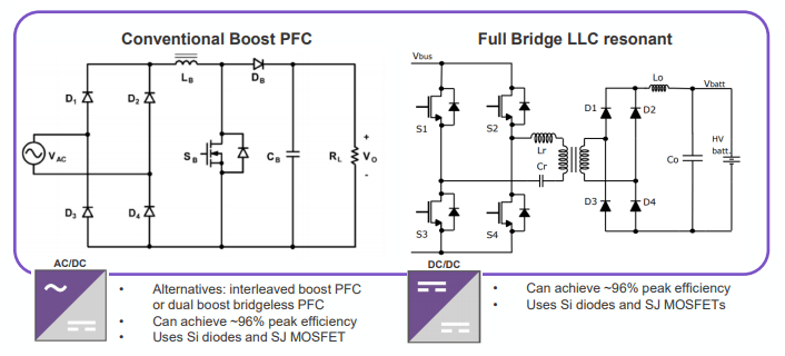
This section will dive into the comparison of the traditional Si-based unidirectional 11-kW OBC and a SiC-based 11-kW OBC. The basic unidirectional Si-based OBC consists of two stages: the conventional boost power-factor–correction (PFC) converter for AC-to-DC conversion and the full-bridge resonant inductor-inductor-capacitor (LLC) resonant converter for DC-to-DC conversion (Figure 3). The first stage provides galvanic isolation and generates the voltage output to follow the charge profile of the EV battery, while the second turns the DC input voltage into a square wave via a switch network and the LLC tank circuit filters out harmonics, thereby providing near-sinusoidal voltage and current waveforms. Alternatives to the conventional boost PFC include the interleaved boost PFC or dual-boost bridgeless PFC. Both the AC/DC and DC/DC stages in this OBC use Si diodes and SJ MOSFET devices whereby both stages can typically achieve a 96% peak efficiency. This ultimately translates to a peak system efficiency of 94%; however, today’s OBC efficiency requirements exceed a 96% peak efficiency in order to meet low cost of operation and emission requirements more rapidly, causing this Si-based option to be non-optimal.
Contemporary solution: SiC-based unidirectional OBC
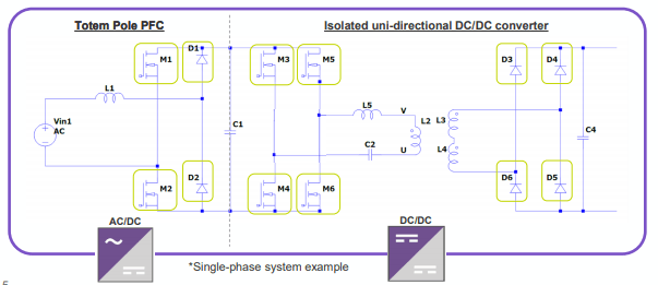
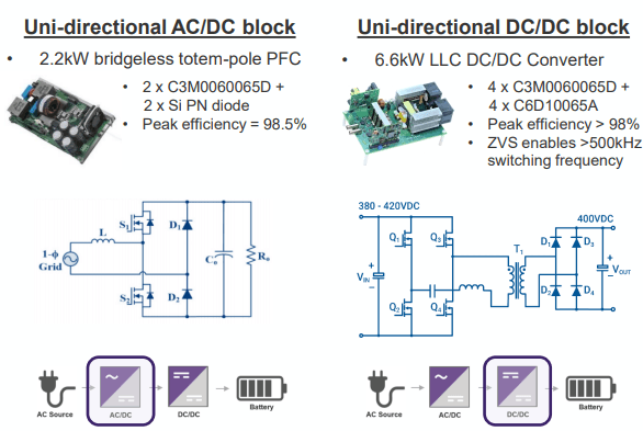
Figure 4 shows the basic building blocks of a SiC-based unidirectional OBC wherein the first stage consists of a totem-pole PFC and the second is an isolated, unidirectional DC/DC converter. This system enables peak system efficiencies of up to 98%, allowing more power to be delivered to the battery with less power wasted, ultimately saving on cost and time. The high power density of the SiC substrate also saves precious space and weight in the EV with a low system cost.
11-kW unidirectional OBC design: Hybrid Si + SiC vs. full-SiC sample designs
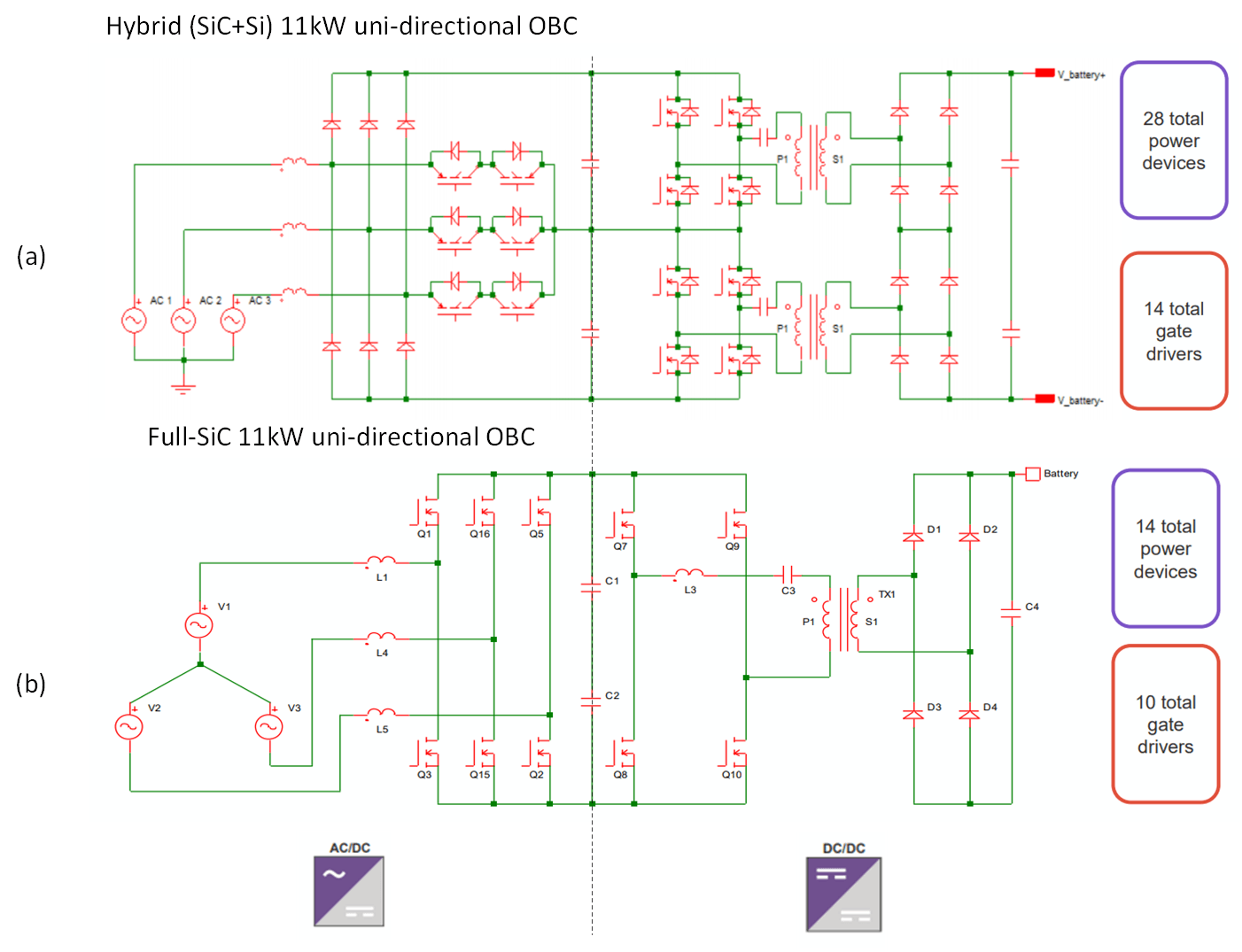
The schematic shown in Figure 5 shows a hybrid Si + SiC implementation as well as a full-SiC design of an 11-kW unidirectional OBC with an input one-phase (90–277 VAC) or three-phase (304–504 VAC) voltage converted to output voltage ranging from 400 to 800 V. The specifications for each of these schematics can be seen in Table 2.
In the hybrid design, the first AC/DC stage contains six SiC diodes and six Si IGBTs as well as six SJ MOSFETs, while the second isolated unidirectional DC/DC stage uses only Si devices (eight SJ MOSFETs and eight Si diodes). To meet the same voltage and current specifications, the full-SiC design utilizes 14 total power devices with six SiC MOSFETs in the first AC/DC stage, as well as four SiC MOSFETS and four SiC diodes in the second isolated DC/DC stage. It can immediately be seen that the power device numbers have been halved, saving on cost and weight for an OBC. The number of gate drivers also dropped from 14 to 10.
Hybrid SiC+Si | ||
|---|---|---|
AC/DC Totel Pole PFC Specs | DC/DC Converter Specs | |
Vin (DC Link Voltage) Vout | 90-277 VAC (1-phase) 304-504 VAC (3-phase) | 380-425 V 480-800 V |
Power Devices | 6 x SiC diodes 6 x Si IGBT/SJ MOSFET | 8 x Si diodes 8 x Si SJ MOSFET |
Fs | 60 kHz | 80-120 kHz |
Full SiC | ||
|---|---|---|
AC/DC Totel Pole PFC Specs | DC/DC Converter Specs | |
Vin (DC Link Voltage) Vout | 90-277 VAC (1-phase) 304-504 VAC (3-phase) | 380-425 V 480-800 V |
Power Devices | 6 x E3M0075120x | 4 x E3M0040120x 8 x E4D10120x |
Fs | 60 kHz | 140-250 kHz |
System cost and benefits comparison
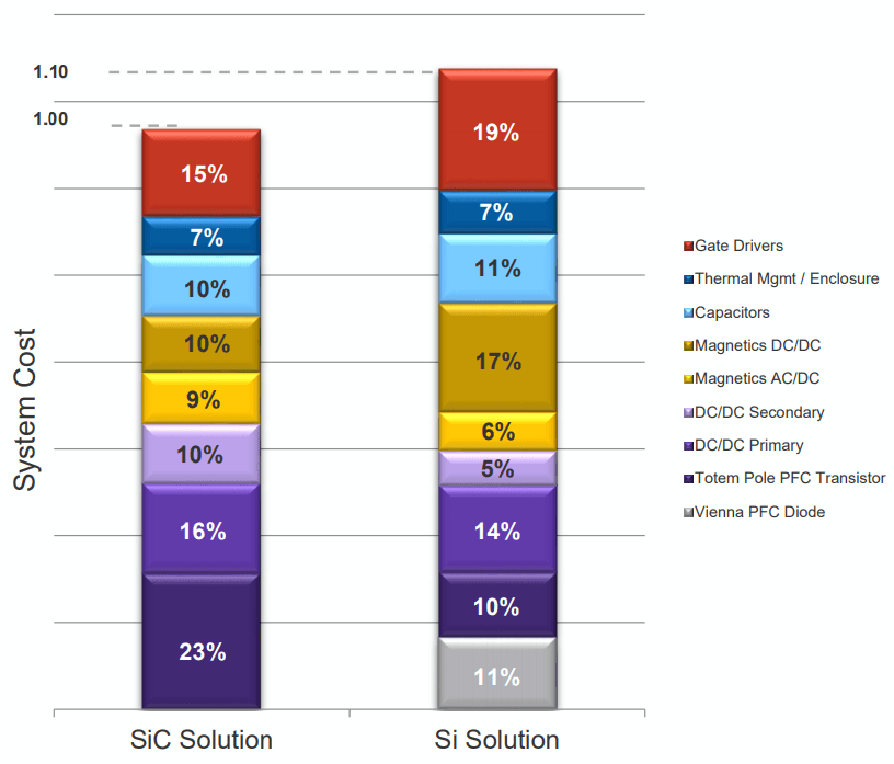
As stated earlier, the drop in the number of active components for the full-SiC allows for a more cost-effective design. A detailed system cost breakdown can be seen in Figure 6. In the first (AC/DC) stage of the full-SiC design, the totem-pole PFC transistors take up the bulk of the cost; however, this cost is offset by the lack of the Vienna PFC diode needed in the hybrid design. Where the full-SiC design ultimately gains its cost advantage is the relatively low amount of gate drivers and the magnetics in the AC/DC stage, leading to a 10% lower system cost.
As shown in Table 2, the switching frequency (fs) is more than double, at 140 kHz to 250 kHz, with conventional system switching frequencies at 80 kHz to 120 kHz. This increase in switching performance allows for smaller inductors which, in turn lowers system cost. The full-SiC implementation of the unidirectional 11-kW OBC not only has a 10% lower BOM cost, but an additional 2% in efficiency that leads to an annual energy savings of nearly $30 for the consumer, all while minimizing the carbon footprint. Table 3 shows the breakdown of the lifetime savings for a SiC-driven OBC compared with the hybrid Si-SiC OBC. Over a 300,000-mile (10-year) lifetime of an EV, a SiC-driven OBC is anticipated to save approximately $435 when including efficiency savings, CO2 savings, and system cost savings. This shows a fundamental cost savings for the OEM and the consumer, all while lowering emissions for the planet.
System Advantage | 11kW uni-directional | 11kW uni-directional |
|---|---|---|
Si | SiC | |
System Cost Savings enclosure, thermal, magnetics, capacitors | 100% | 90% <$16 |
Power Density OEM-specific $/liter | ca. 2kW/L | ca. 3kW/L |
System Efficiency (Operational Savings) 0.55k (0.43)Wh/100km * 30,000km/y * $0.36/kWh | 95% ./. | 97% $26/year |
SiC-driven CO2 Savings 3000k km lifetime * 400g/kWh, 0.44 (0.43)kWh/100km * $72/t | ./. | $31 |
SiC-driven Net Lifetime Savings (systems cost savings + operational savings + CO2 savings) | ./. | ~$435 |
The advantages of choosing Wolfspeed for your next SiC design
Wolfspeed’s SiC system expertise helps accelerate innovation and time to market for customers with over 30 years of manufacturing experience of SiC chips. This legacy has led to over 7 trillion field hours of devices already installed, over 17 years of SiC diode and MOSFET production, and the largest market share in SiC technology — all with the intent to increase capacity of SiC-based products 30× by 2024. The inherent system expertise allows for superior engineering, and applications support streamlines the design, prototyping, and implementation process for a reliable finished product. Both the AC/DC stage and DC/DC stage for unidirectional OBCs are already commercially available in a full-SiC implementation (Figure 7). This allows designers to readily employ SiC-based components in their OBC system, all while maintaining an efficiency beyond 98%, while saving on precious EV space and costs.
References
- A. Khaligh and M. D’Antonio, “Global Trends in High-Power On-Board Chargers for Electric Vehicles,” in IEEE Transactions on Vehicular Technology, Vol. 68, No. 4, pp. 3306–3324, April 2019.