Wolfspeed WolfPACK™ Power Module Platform: Accelerating Fast-Charger Development
Article
The FM3 platform simplifies the design of converter power stages, reducing development time and cost.
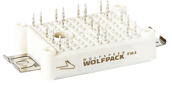
Wolfspeed is delivering a new family of cost and performance optimized housings which simplify the adoption of Silicon Carbide (SiC) MOSFETs. The Wolfspeed WolfPACK module family uses a fixed interval pin-grid for rapid development of alternate configurations, and devices are currently available in half-bridge and six-pack configurations. With no baseplate, the module substrate is cooled directly, and the standard module height allows reuse of thermal management solutions between converter designs, even when using alternate module configurations.
Fast-Charging

As electric vehicles (EVs) fill an increasing percentage of the automotive market, the demand for on-route fast charging will continually increase. In the race to match internal combustion engine (ICE) refueling time, these chargers will require increasing power specifications. Delivering high power without excessively large cables requires relatively high output voltage. The combination of design requirements makes SiC power modules an ideal candidate in fast charger design.
In this design exercise, several requirements are considered which are appropriate for commercial/municipal fast charger implementations.
- Three-Phase, AC Input
- Isolated architecture (for safety purposes)
- 60 kW+ Output Power per Converter Cell
- Regulated DC output, up to 800 V
By selecting 60 kW per converter cell, each converter cell is capable of fast charging a vehicle alone. However, multiple cells can be used in parallel to achieve higher power levels for even faster charging.
Additionally, the converter building blocks discussed in this application are intended to be extensible to alternate systems. To maximize the opportunities for these systems, the ability to allow for bidirectional power flow was added to the converter requirements.
Design Space
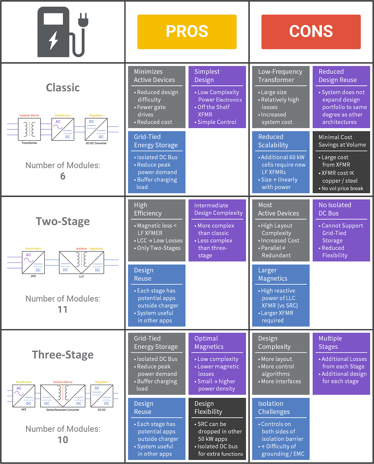
There are many potential architectures which could be developed to meet the design requirements of DC fast charging. In order to evaluate the potential design space, several candidate architectures are reviewed at a high level.
Low-Frequency Transformer

The traditional solution for creating a regulated DC bus is to first reduce the voltage with a 50/60 Hz transformer, passively rectify, and finally add a regulating converter (such as a buck converter) to the intermediate-DC bus. While the performance of such an architecture can be improved with an active front end (AFE) rectifier, this does not address the primary disadvantage of the architecture. Specifically, a 60 kW, 50/60 Hz transformer adds significantly more size, cost, and losses than a high frequency transformer.
Two-Stage Architecture

The two-stage architecture eliminates the low frequency isolation transformer by using an isolated converter topology which has a regulated output. By including both regulation and isolation a single converter, the low frequency transformer can be eliminated while minimizing total system complexity and number of active devices.
Active Front End
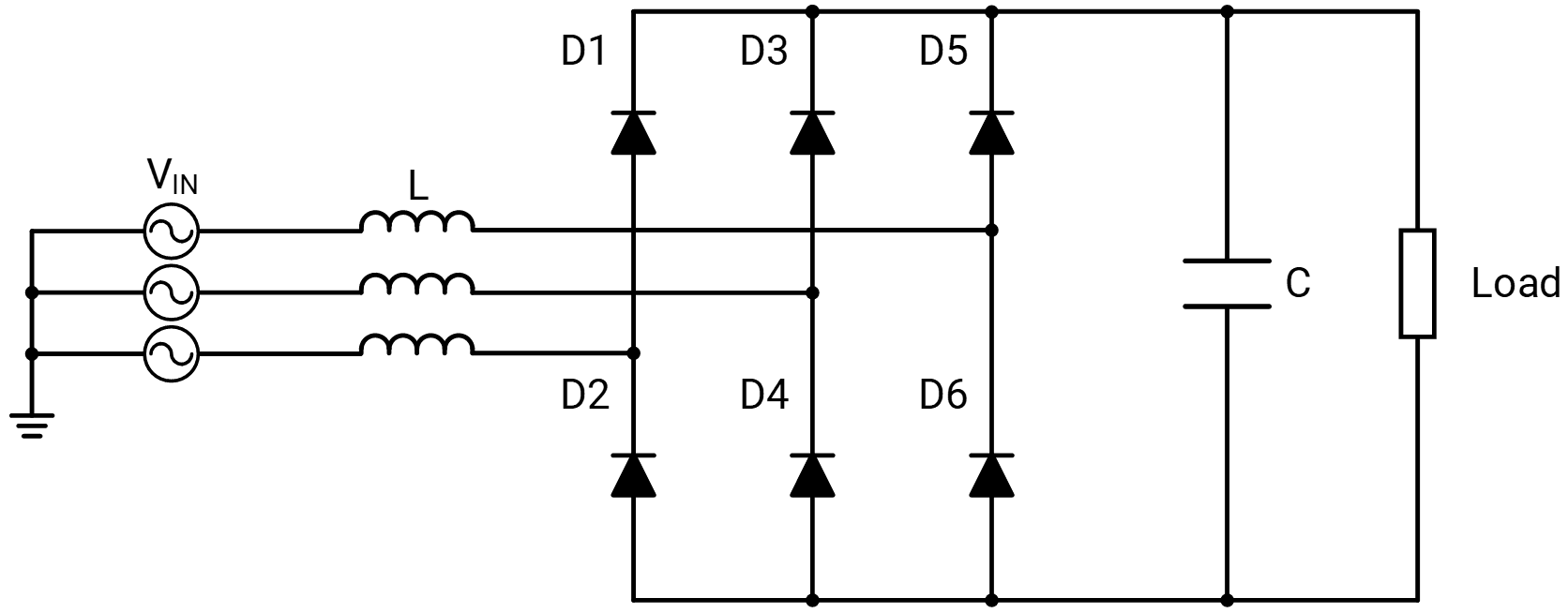
In DC fast charger applications, input power is generally supplied in the form of three-phase AC. The schematic above shows the general design for a three-phase, full-wave passive rectifier, which can be used to create a DC bus.
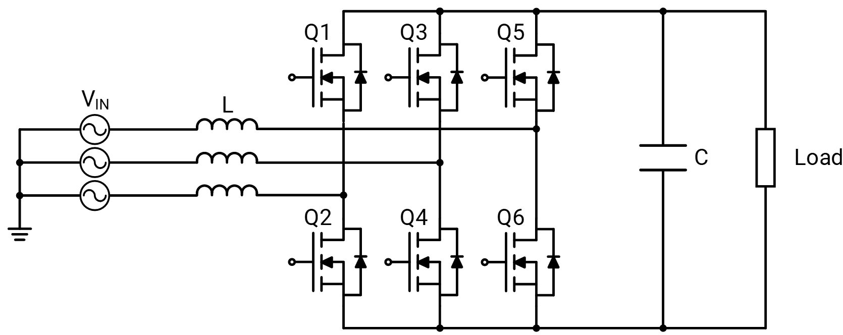
Replacing the passive diodes with active components, such as the MOSFETs shown above, can substantially improve converter efficiency by eliminating the diode conduction losses `(V_f xx I)` in exchange for the MOSFET ohmic losses `(R_(DS(on))xxI^2)`, which are typically lower. Additionally, when coupled with the correct control scheme, active devices allow for bidirectional energy flow which is highly beneficial in certain applications.
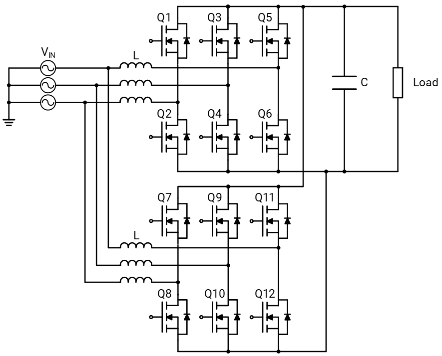
When the power / current requirements of the rectifier’s load exceed the current capability of the active devices, multiple devices can be placed in parallel to meet the demand. However, it is beneficial to interleave additional rectification stages instead. This is because the rectifier’s performance can be improved at a similar component cost. Specifically, the interleaved stages lead to reduced ripple current for a given inductor size, improves converter power factor, and can improve fault tolerance. The above schematic shows two interleaved phases; however, more phases can be added as necessary to reach the converter power requirements.
LLC Converter
The example two-stage architecture uses an LLC resonant converter, but other isolated topologies with regulated outputs could be considered (for example, the phase-shifted full bridge). The LLC converter (named for the components in its resonant tank) has several advantages such as the low number of active components, ability to achieve zero voltage switching (ZVS), and relatively simple controls. Additionally, the transformer turns ratio can be used to control the output voltage range available to converter.

When operating a converter with ZVS, there is a substantial reduction in switching losses (as the switching losses of the active devices are correlated to the blocking voltage at the switching event). Therefore, converters like the LLC can be highly efficient.

The schematic above shows the LLC converter modified to use active rectification on the secondary (replacing the 4 diodes with MOSFETs), which can lead to improved efficiency due to reduced conduction losses. This also allows the topology to enable bidirectional power flow, as discussed in the overarching goals for these converter designs.
The LLC also has some disadvantages. These are primarily related to the method of regulation, which requires changing the switching frequency (rather controlling a duty cycle as in traditional PWM converters). One consequence is that the load cannot be arbitrary and must be considered during the design of the resonant tank. Realistically, the load current bound can be determined in the design phase of fast charging applications so this disadvantage is minor. Another consequence of frequency control is the implications to electromagnetic-interference (EMI). For fixed frequency converters, a narrow band EMI filter can be designed to strongly suppress EMI near the switching frequency. In variable frequency converters, EMI filters require a broader range of suppression. Finally, the LLC will generally have a large reactive component to the transformer current, which increases reactive energy. Reactive powers three times higher than the real transformer power are feasible, greatly increasing the required transformer power capability to handle the associated reactive energy.
Three-Stage Architecture

The three-stage architecture divides the functions of isolation and regulation between two converters, which increases the complexity of the system. Despite this, the three-stage architecture has several specific advantages over its two-stage counterpart. The selection of converter subsystems can be individually optimized, for example. The most important advantage of the three-stage architecture is the addition of an isolated DC bus, which can be used for grid-tied storage and load buffering.

A factor that may be important in fast-charger design is peak power available from the grid. If the desired output power of the charging infrastructure is beyond the designed peak input power to the system, load balancing may be required using grid tied energy storage. This allows energy to be pulled slowly between charging cycles and delivered rapidly when an external load is applied. In such scenarios, the amount of energy storage is quite high, so technologies other than battery storage may be necessary. An alternative use of this architecture could leverage a smaller amount of storage to manage short peak peaks and smooth out overall grid demand by reducing the rate of change in the power pulled from the grid. If the grid tied converter and isolation stage are designed to allow bidirectional energy flow, this grid tied storage can also be used by operators to assist with peak grid demand when the charger is not in use.
Isolation Converter: Series-Resonant Converter
The LLC converter presented in the two-stage architecture can be modified into an isolated series-resonant converter (SRC) by altering the control scheme. SRCs can achieve both ZVS and zero-current switching (ZCS), which eliminates switching losses entirely. However, the output cannot be regulated while maintaining both ZVS and ZCS. This creates the need for a third DC-DC regulation stage but as such a stage was already necessary for the isolated grid-tied energy storage, the SRC is appropriate in this architecture. In order to reduce conduction losses and allow bidirectional energy flow, an active secondary is selected.

As mentioned previously, the primary downside of SRCs is the unregulated output (when achieving both ZVS and ZCS). However, since an additional converter was already necessary for output regulation while maintaining an isolated bus, the only implication for the architecture is that the voltage on the isolated bus must be allowed a wider voltage range, which should be considered in the design of the regulating converter and energy storage element. In this schematic, it is shown that the resonant tank can be split, which may be desirable for cost savings, if two smaller capacitors / inductors are cheaper than one larger.
DC-DC Stage
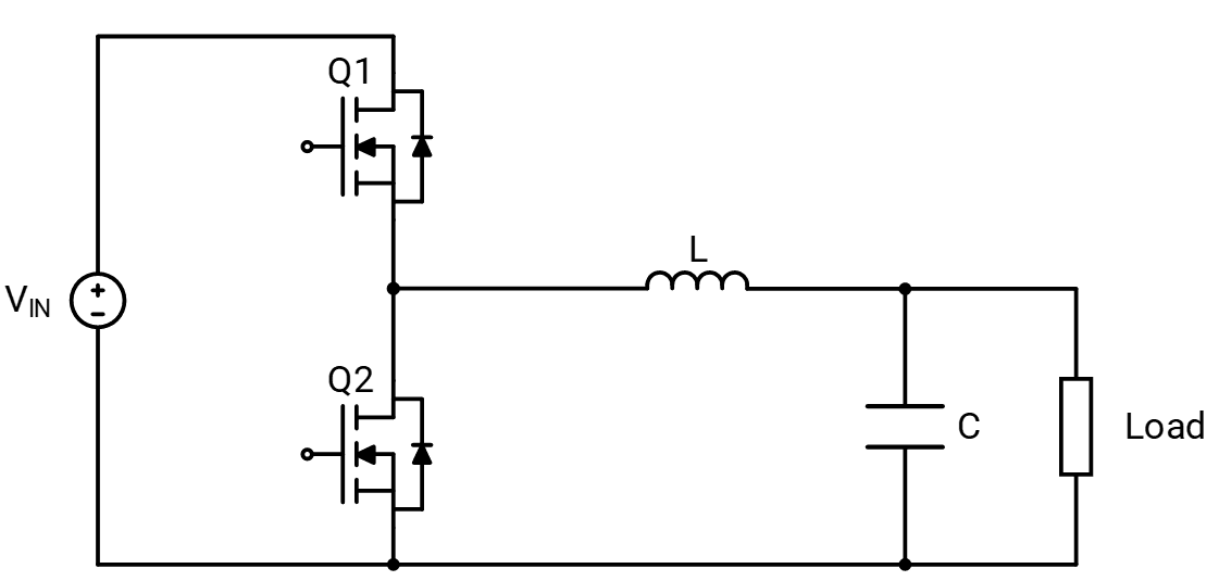
Buck converters represent an extremely simple solution for regulating the output of the three-stage architecture. By maintaining an intermediate bus voltage greater than the output, the regulation can be accomplished without the need for voltage boosting. In order to minimize conduction losses, an active switch is used in the lower position, Q2 (instead of a diode). This switch is gated-on asynchronously from Q1 with deadtime required to prevent shoot-through.
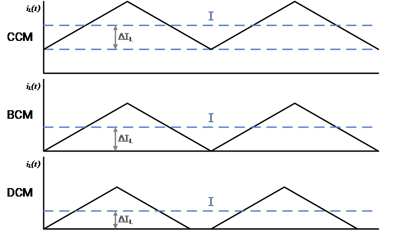
The diagram above shows three modes of operation in the buck converter, which are determined by the output current through the load inductor. Continuous conduction mode occurs when the average output current is greater than the current ripple. Similarly, discontinuous condition mode occurs when the ripple current is greater than the average, causing the current through the low-side switch to drop to zero during its active period. Boundary conduction mode is found at the critical condition when the low-side switch current reaches zero at the end of it’s on period.
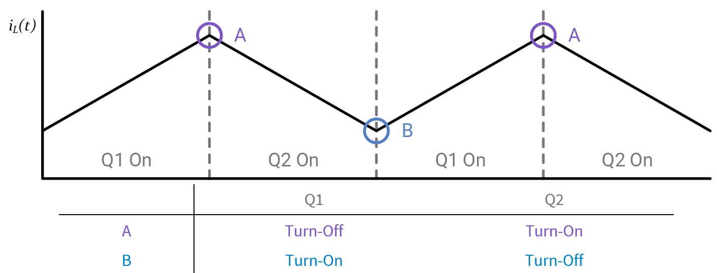
Annotations are added to the waveform to highlight the active switch and transient events (although it is simplified by ignoring dead-time). At the events labeled “A,” the high side switch turns off, and current flows through the low-side position to prevent discontinuity in the inductor current. Similarly, when the end of the switching cycle is reached at “B,” the low-side device turns off while the high-side device turns on. It would be advantageous for event “B” to occur at the same moment the switch current reaches zero as this would lead to ZCS of Q1 with elimination of Q1 turn-on losses. Additionally, and perhaps even more importantly, ZCS of Q2 would eliminate reverse recovery and the associated voltage overshoot. This enables very aggressive gate resistor values that would not be achievable in CCM (due to aforementioned voltage overshoot at diode recovery). Therefore, BCM operation of a buck converter can lead to very high efficiency with reduced device stress. To maintain BCM, switching frequency can be controlled in response to the load current (as BCM is a function of switching frequency, duty cycle, and load).
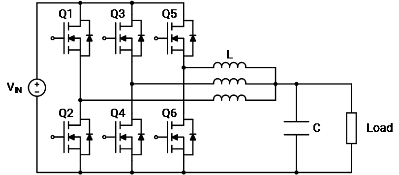
Due to the relatively high output current of a 60 kW DC fast charger (150 A at 400 V, for example), multiple transistors in parallel are likely required (which could be achieved with a high current power modules). Rather than operating multiple transistors in parallel, additional converter phases can be interleaved to improve converter performance for a similar component cost (albeit while requiring more gate outputs from the controller). By interleaving multiple buck converter phases, the current ripple on the output can be reduced (which is helpful to offset the relatively high current ripple required to operate in BCM). Similarly, this allows the filter component size to be reduced and improves the converters power factor. Additionally, by deactivating phases at light load, switching losses can be reduced for improved efficiency.
Similar to the LLC, controlling the switching frequency of the buck converter increases the complexity of EMI filter design. One advantage for the buck converter, however, is that it is operated on an isolated DC bus, giving it electrical separation from the grid and likely reducing the EMI filter requirement.
Architecture Implications on Magnetics
AFE Filter Inductors
The magnetics design for the AFE is relatively simple as the converter merely requires an appropriate filter inductor to maintain a suitable current ripple (although the more core complex task of determining EMI filter requirements for the total system was not considered in this exercise). The AFE requires one inductor per phase and achieving a good compromise between inductor and capacitor size requires a ripple current value of 10 - 30% of maximum inductor current.
LLC Transformer
The design of the LLC transformer is the most complex of the magnetic design tasks for the converter topologies discussed in this assessment. As mentioned previously, the large component of reactive power is also likely to make this transformer larger than one designed for the SRC (albeit much smaller than a 60 Hz transformer of similar power rating). Discussing the design process for such frequency controlled resonant-tank converters is considered out of scope for this white paper, but substantial resources are available on the topic.
Series-Resonant Transformer
The design of a transformer for SRCs is somewhat simpler than the LLC transformer. This is in part because the symmetric design, in part because the unregulated output of the converter simplifies the impedance requirements of the resonant tank, and in part because the lower reactive power component reduces the sizing requirement of both copper and ferrous components. The design of SRC transformers requires minimization of the leakage inductance so that the impedance of the resonant tank is relatively small compared to the apparent load resistance. The magnetizing current must be large enough to recharge the output capacitance of the primary and secondary transistors, otherwise ZVS and ZCS cannot be maintained (and switching losses would occur). Unlike the LLC transformer, the reactive power of the SRC transformer should generally be on the order of the real power.
Buck Converter Filter Inductors
Since the buck converter is operated in BCM, the inductor size can be determined from the need for current ripple to be twice the mean inductor current. First, the minimum output voltage allowed for full power must be designed as this will determine the maximum current (for example, 125 A at 400 V). Generally, the equation,
can be used to calculate the inductor value, where tonton is the period where the high-side switch, Q1, is on. This can be calculated from the duty cycle (which is calculated from the ratio of output to input voltage) and approximate switching frequency, which can be selected as part of the design process. Of course, this switching frequency will be altered by the control to maintain BCM, but the range of frequencies will be determined by the load current and inductor value.
Simulation Studies
Wolfspeed provides simulation models which can be leveraged to accelerate the design process. For users who do not own a PLECS license, several of the simulations described can be run using Wolfspeed’s SpeedFit 2.0 Design Simulator™:
For users with access to PLECS Blockset or PLECS Standalone, Wolfspeed offers models for all its discrete devices and power modules, available at:

The MOSFET models are developed to accurately predict turn-on and turn-off losses across junction temperature, across drain to source current, across bus voltage, and across gate resistance (where turn-on and turn-off gate resistors can be selected separately). Likewise, conduction losses are modeled over junction temperature and drain to source current. Finally, the transient thermal impedance of the MOSFET junction to case is modeled with a thermal network.
Models of the MOSFET body diodes are also provided which include both conduction losses and transient thermal impedance.
Rectifier: Active Front End
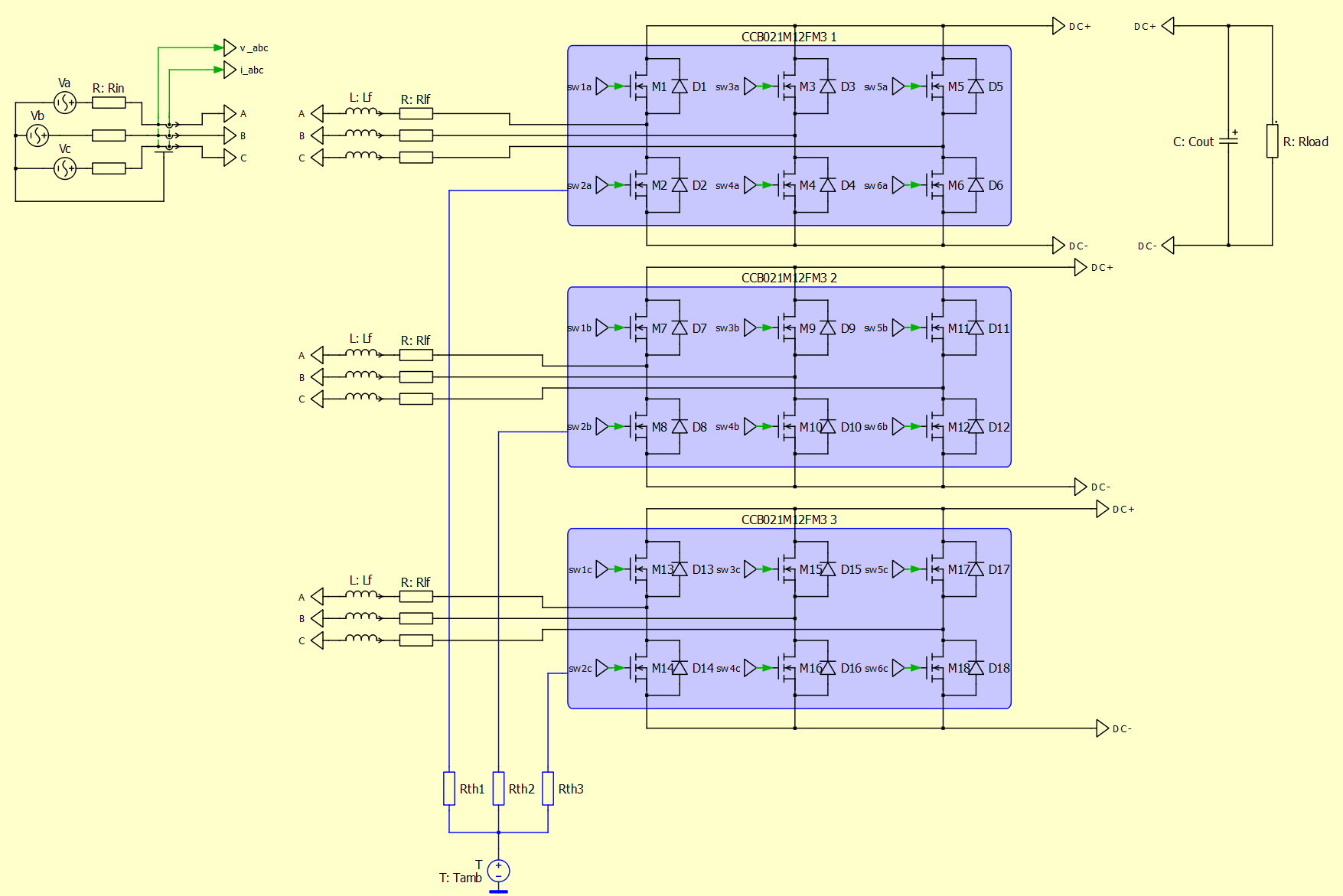
The simulation model for the AFE in PLECS is shown above, which uses three interleaved phases. Each phase uses the CCB021M12FM3 6-pack module.
The primary parameters for the simulation are:
Power Module | Input Voltage | Output Voltage | Thermal Impedance, Case to Ambient | Ambient Temperature |
|---|---|---|---|---|
CCB021M12FM3 | 480 V AC | 800 V | 0.43 °C/W | 65 °C |
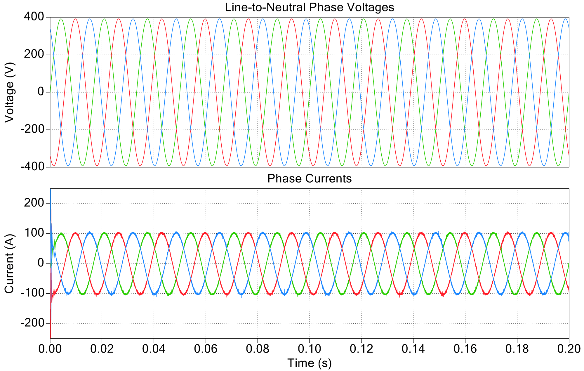
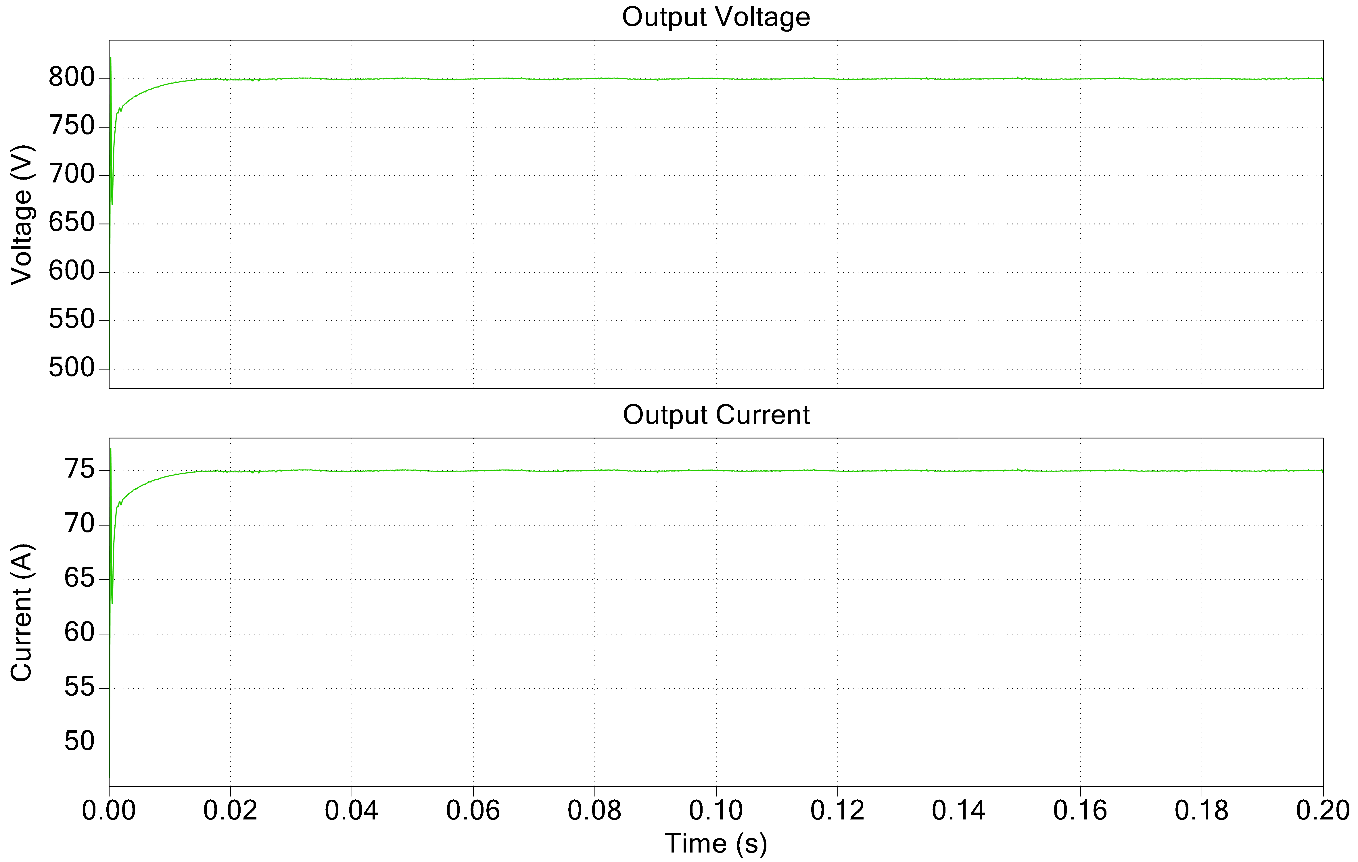
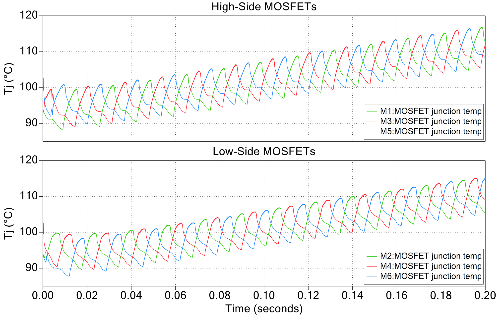
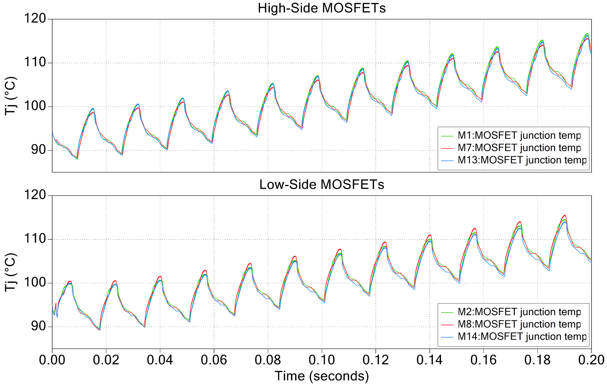
Based on the simulation results, modules required:
In order to be thermally stable at 60 kW output, two interleaved modules may be possible if very high-performance cooling is employed. However, the additional phase allows for the possibility of air cooling, provides improved current ripple performance, and allows for output power beyond 60 kW. Therefore, reallocating some of the budget from thermal management to additional SiC can lead to improved system performance.
Two-Stage Architecture

The simulation model for the LLC in PLECS is shown above, which uses two modules in parallel for each leg of the full bridge. Each module is the CAB011M12FM3 half-bridge power module.
Note that in this simplified simulation model bidirectional power flow has not yet been modeled. Instead, diodes are used without a thermal model. It is assumed that achieving 60 kW in the reverse direction will require the same configuration of modules for the secondary as the primary.
The primary parameters for the simulation are:
Power Module | Input Voltage | Output Voltage | Thermal Impedance, Case to Ambient | Ambient Temperature |
|---|---|---|---|---|
CAB011M12FM3 | 480 V AC | 800 V | 0.43 °C/W | 65 °C |
Resonant Tank:
Lr | Lm | Cr | Turns Ratio | Pout |
|---|---|---|---|---|
2.11 μH | 100 μH | 1.2 μF | 1:1 | 60 kW |

Based on the simulation results, modules required:
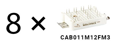
Simulation results indicated that a two-module full-bridge was insufficient for reaching 60 kW output power in the LLC, and thus additional modules were required in parallel. Even with 4 modules, the LLC still reaches nearly TJ,max (150 °C) at 60 kW output power.
While the simulation above shows only 4 half-bridge modules (and 4 diodes on the output), in order to reach 60 kW in the reverse power flow direction, 4 additional modules will be required on the secondary side, therefore, the LLC requires 8 modules in total to meet the design requirements.
Three-Stage Architecture
Simulation analysis of SRC

The simulation model for the SRC in PLECS is shown above, which uses a single module for each leg of the full bridge (primary) and active rectifier (secondary). Each module is the CAB011M12FM3 half-bridge power module.
The primary parameters for the simulation are:
Power Module | Input Voltage | Output Voltage | Thermal Impedance, Case to Ambient | Ambient Temperature |
|---|---|---|---|---|
CAB011M12FM3 | 480 V AC | 800 V | 0.43 °C/W | 65 °C |
Resonant Tank:
Lr | Lm | Cr | Turns Ratio | Pout |
|---|---|---|---|---|
2.11 μH | 100 μH | 1.2 μF | 1:1 | ~100 kHz |
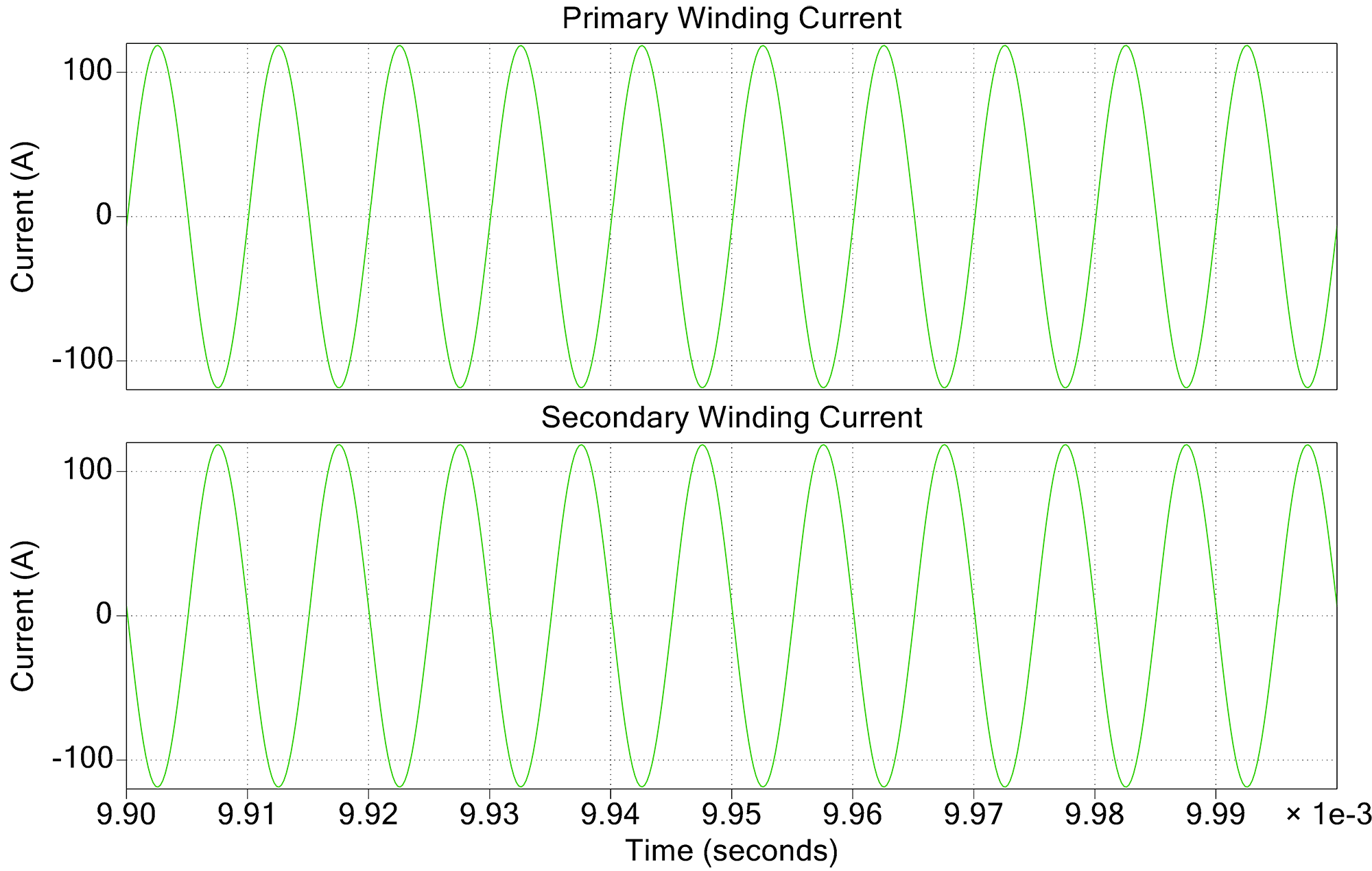
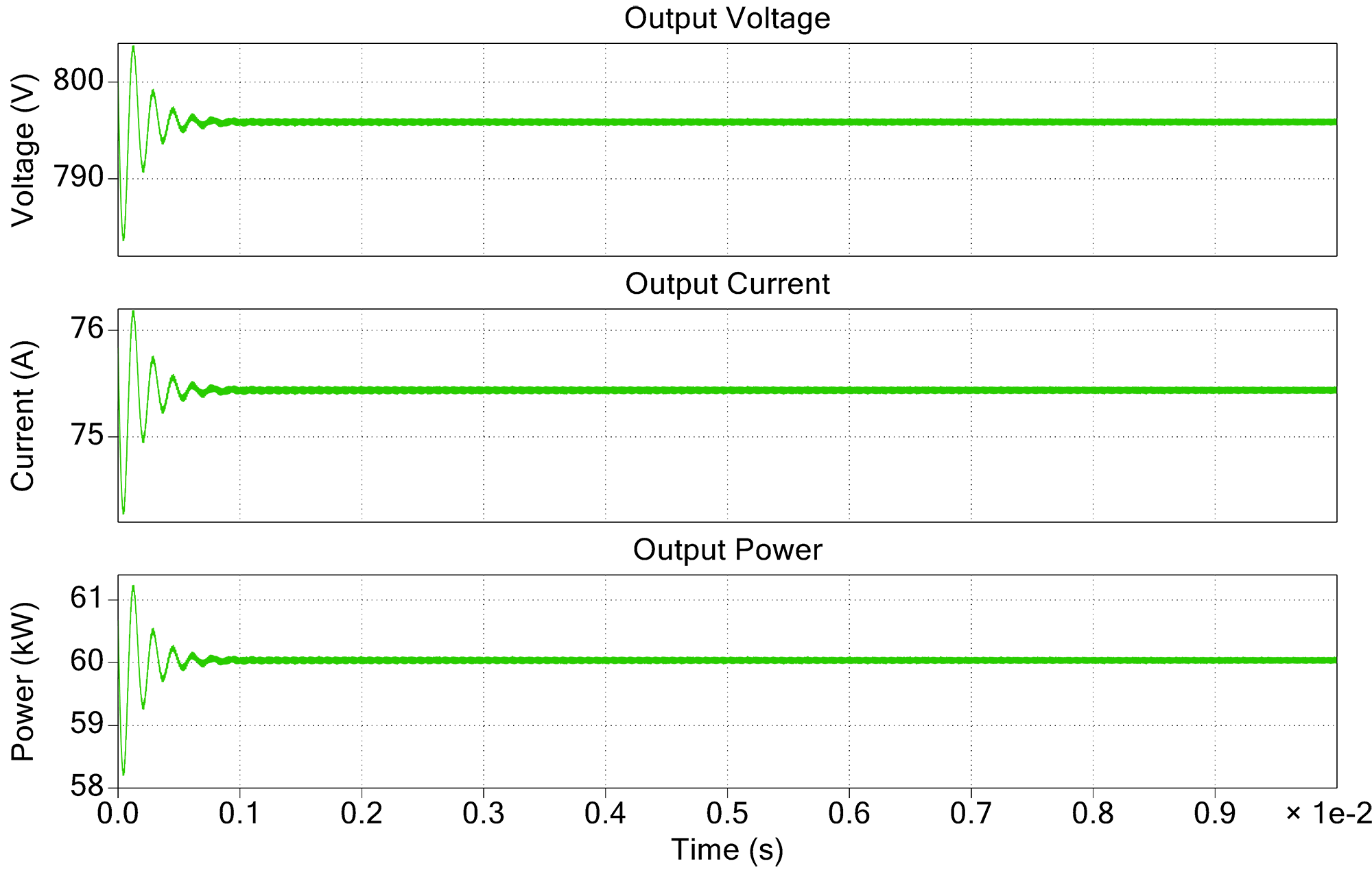
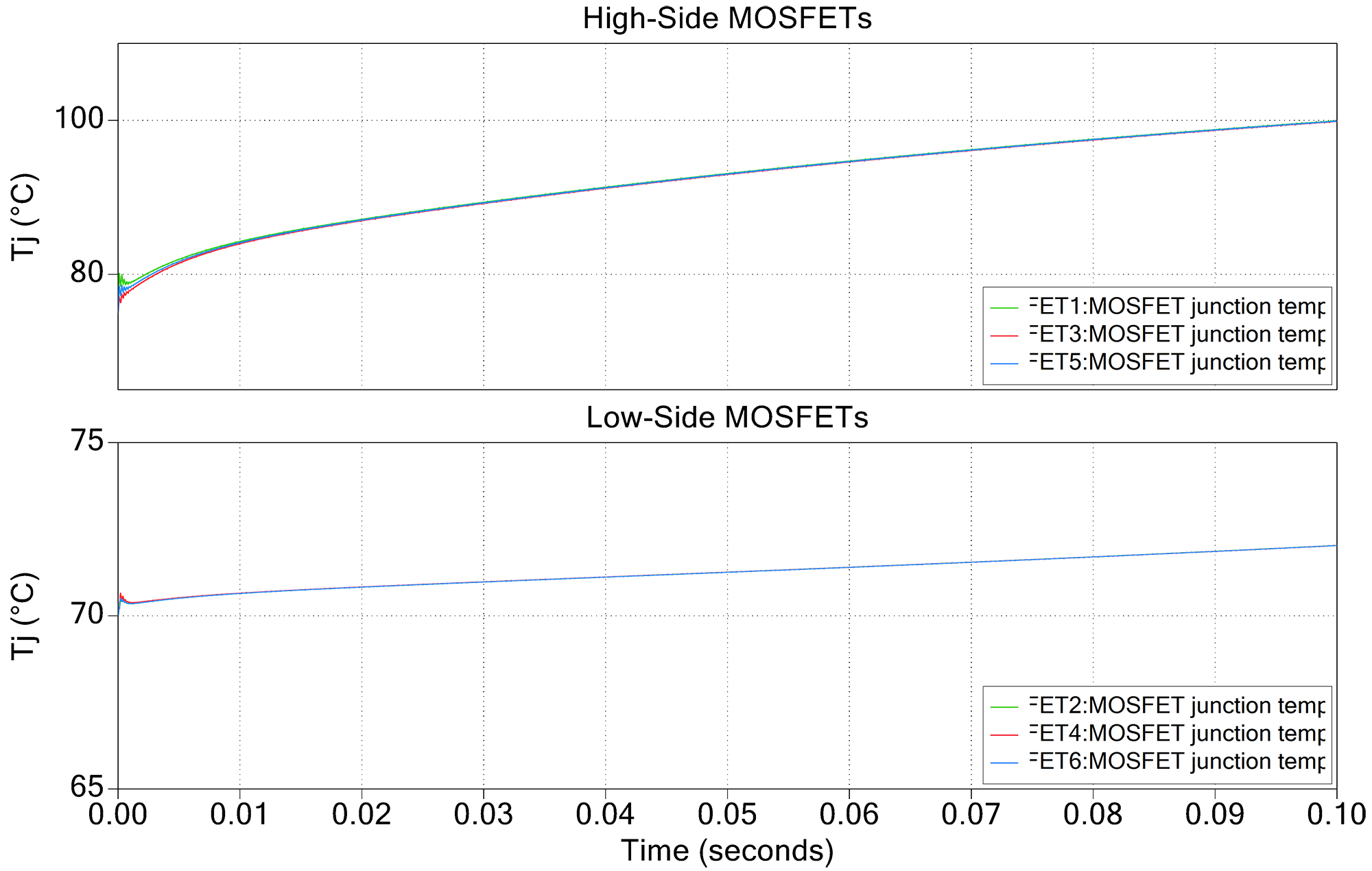
Based on the simulation results, modules required:
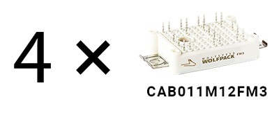
Due to negligible switching losses when achieving ZVS and ZCS, the SRC can easily achieve 60 kW at a reasonably low junction temperature. These early results indicate that there is more head room remaining in this design.
Simulation analysis of DC-DC
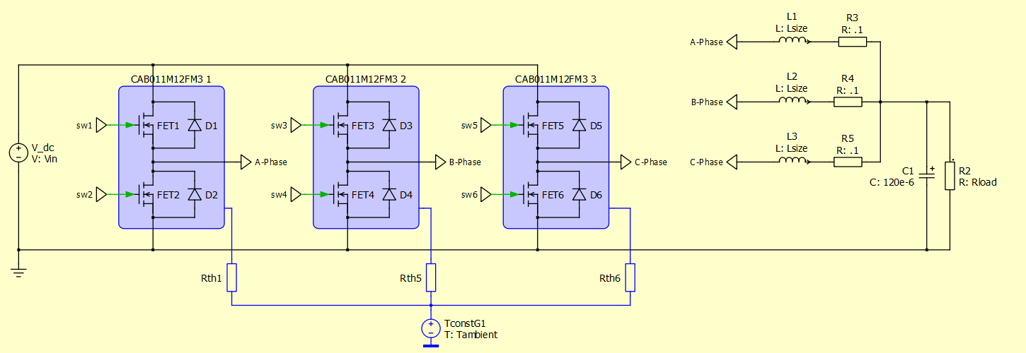
The simulation model for the Interleaved buck converter in PLECS is shown above, which uses three phases. Each module is the CAB011M12FM3 half-bridge power module.
The primary parameters for the simulation are:
Power Module | Input Voltage | Value of Each Filter Inductor | Thermal Impedance, Case to Ambient | Ambient Temperature |
|---|---|---|---|---|
CAB011M12FM3 | 800 V AC | 25.8 μH | 0.43 °C/W | 65 °C |
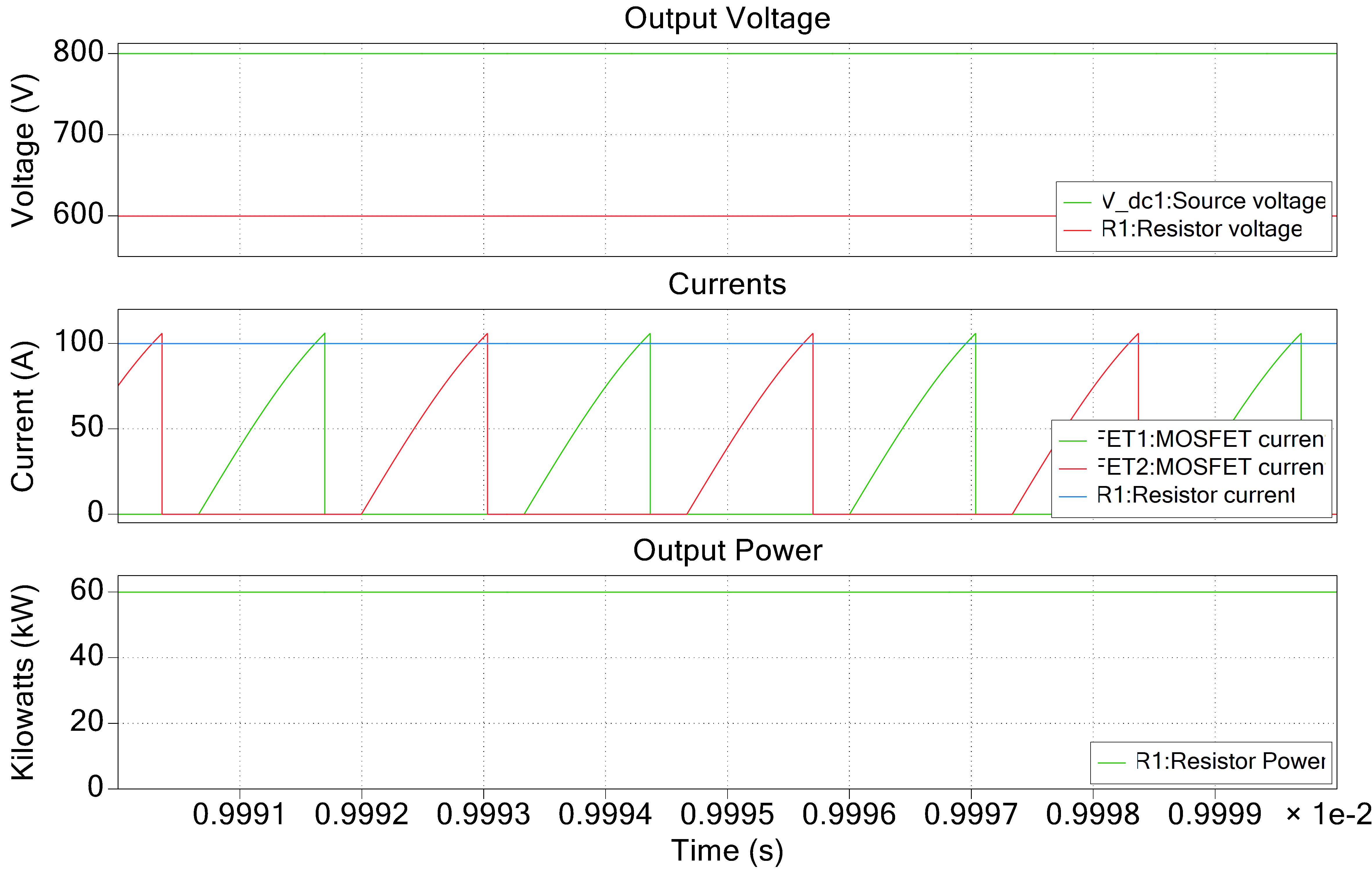
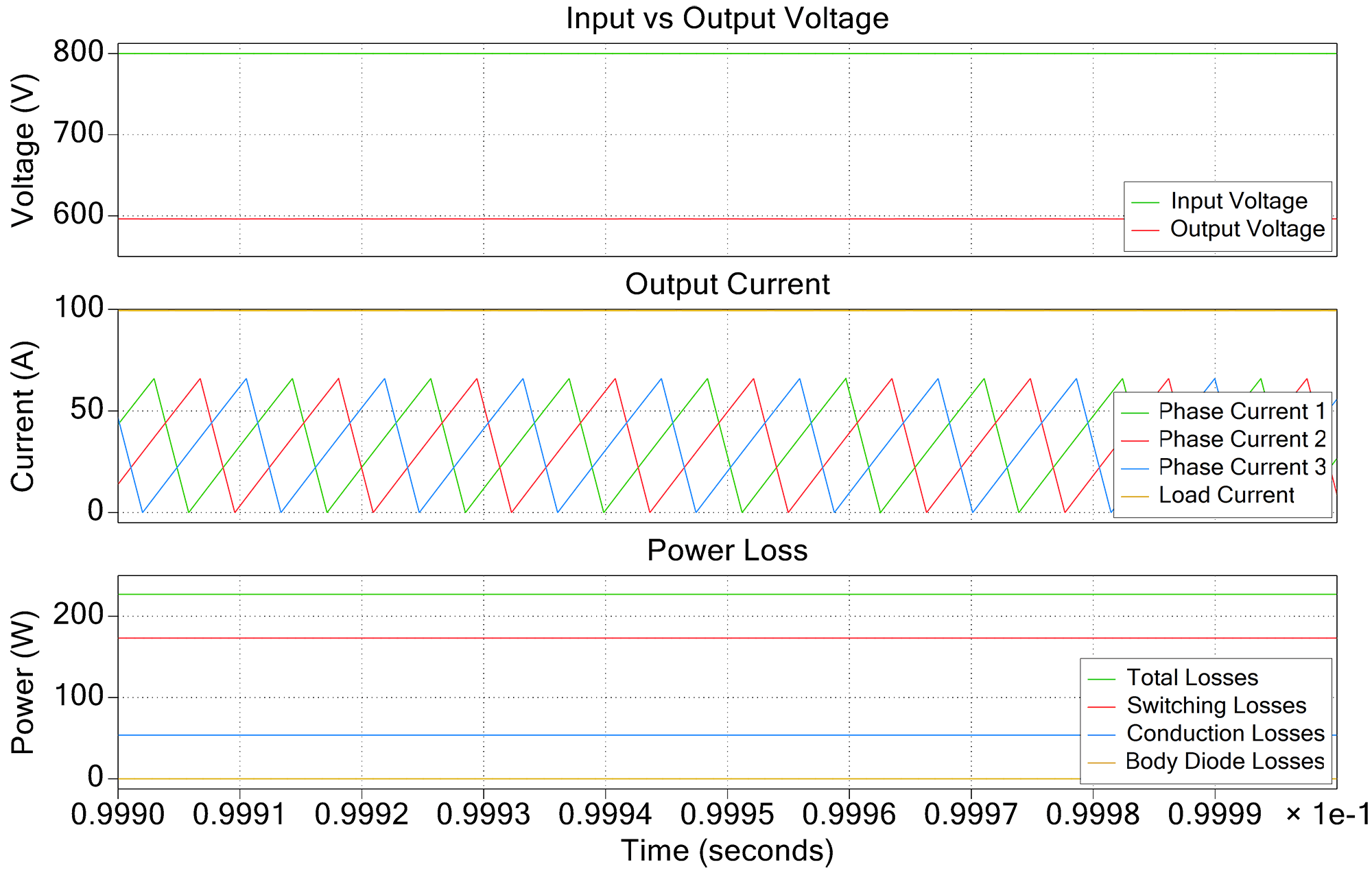
In the simulation shown above, the interleave buck converter is operated for a fixed conversion ratio and output power. Demonstration waveforms were generated at the following conditions:
Input Voltage | Output Voltage | Output Power | Output Current | FSW1 |
|---|---|---|---|---|
800 V | 600 V | 60 kW | 100 A | 88103 Hz |
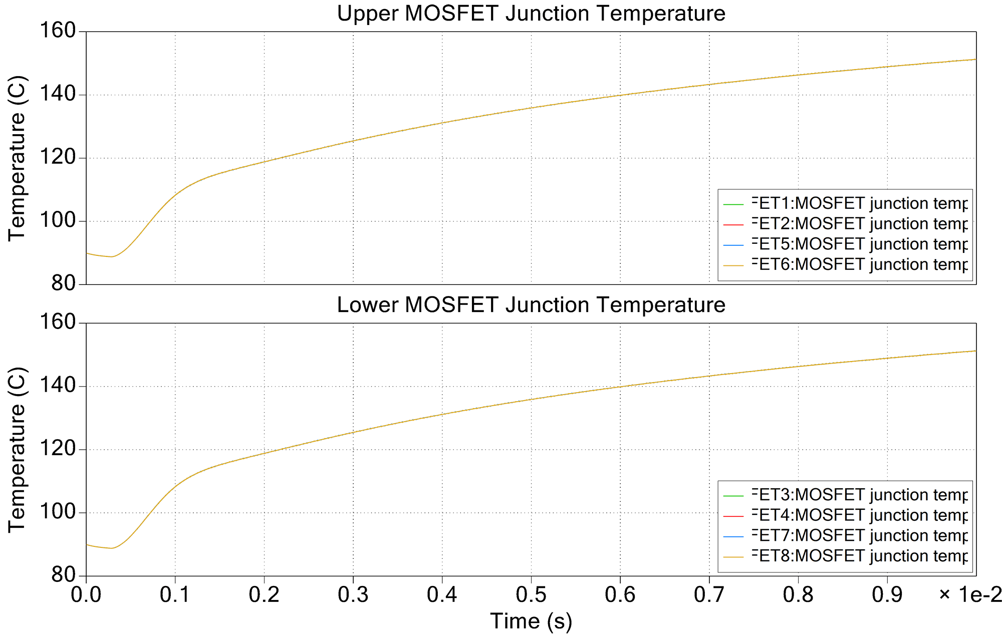
Based on the simulation results, modules required:
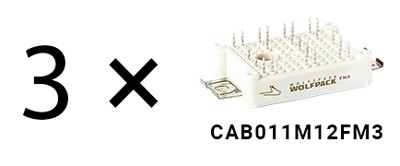
Due to low switching losses related to the aggressive Rg (allowed by BCM operation), the 3-phase interleaved buck converter can easily achieve 60 kW at a reasonably low junction temperature. In addition to the thermal requirement, however, three modules were mandated to meet the current requirements at lower output voltages.
Comparison between Architectures
