Use Silicon Carbide Based MOSFETs to Improve Power Conversion Efficiency
Article
The trends of higher power requirements, regulatory mandates, and standards on efficiency and EMI issues are driving the need for power supplies to use switching power devices due to their greater efficiency and wider operating range. At the same time, designers are under constant pressure to reduce cost and save space. In the face of these requirements, what’s needed is an alternative to classic silicon (Si)-based MOSFETs.
Silicon Carbide (SiC) has emerged as a clear option now that it has matured and is in its third generation. SiC-based FETs offer many performance advantages, particularly with respect to efficiency, greater reliability, fewer thermal management issues, and smaller footprint. These apply across the power spectrum and do not require a radical change in design techniques, although they may require some adjustments.
This article provides a brief comparison of Si versus SiC, introduces examples of SiC devices from Wolfspeed, and shows how to start designing with them.
SiC versus Si MOSFETs
First, it’s important to be clear about technology and terminology: SiC-based FETs are MOSFETs, just like their silicon predecessors. In the broad sense, their internal physical structures are similar, and both are three-terminal devices with source, drain, and gate connections.
The difference is as their names indicate: SiC-based FETs use Silicon Carbide as their base material rather than silicon alone. Many in the industry refer to them as Silicon Carbide devices and leave out the MOSFET part. This article will refer to them as SiC FETs.
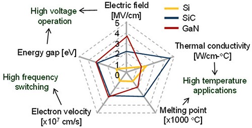
Why use a SiC compound as the material? For various deep physics reasons, SiC has three major electrical characteristics that differ significantly from silicon, with each bringing operational advantages; there are other, more subtle ones as well (Figure 1).
They are:
- Higher critical breakdown electric field voltage of about 2.8 megavolts per centimeter (Mvolts/cm) versus 0.3 Mvolts/cm, so operation at a given voltage rating is possible with a much thinner layer, greatly reducing on-resistance.
- Higher thermal conductivity, enabling higher current density in a cross-sectional area.
- Wider bandgap (the energy difference (in eV) between the top of the valence band and the bottom of the conduction band in semiconductors (and insulators) resulting in lower leakage current at high temperatures. For this reason, SiC diodes and FETs are often referred to as wide bandgap (WBG) devices
As a result, in approximate terms, SiC-based devices can block voltages up to ten times higher than silicon devices, and can switch about ten times faster with an on-resistance of half or less at 25°C. At the same time, their very ability to operate at much higher temperatures of 200°C versus 125°C eases thermal design and management.
Gate driver critical to realizing benefits
A power device does not function without its gate driver, which translates low-level digital control signals into the needed current and voltage signals along with the timing required by the power device (while also providing some protection against most types of external faults). For SiC FETs, the driver must include additional functions in order to provide the following:
- Minimize conduction and switching losses as well as gate losses. These losses include turn-off and turn-on energy, the Miller effect, and gate drive current requirements. Turn-off energy is a function of gate resistance and gate-to-source voltage in the off state. To reduce these, more current must be drained from the gate. One of the ways to do this is for the driver to apply a negative bias to the gate voltage during the turn-off time. Similarly, turn-on energy is reduced by reducing the gate resistance.
- Minimize the Miller effect and its negative consequences, where parasitic capacitance may cause inadvertent turn-on under some circumstances and application configurations. This Miller-induced turn-on increases the reverse recovery energy and adds to losses. One solution is for the driver to have what is called a Miller clamp-protection function, which controls the drive current during switching of the power stage.
- Provide needed sink and source current at appropriate voltages. SiC devices generally require a higher positive bias gate drive (+20 volts) than silicon MOSFETs to minimize losses; they may also need a negative OFF gate voltage between -2 to -6 volts. The required gate current is determined by the usual calculations based on gate charge (Qg), VDD, drain current ID, gate-to-source voltage, and gate resistance, and is typically on the order of a few amps. This current must have adequate sink and source ratings at a slew rate commensurate with the switching speed of the SiC FET
- Model and minimize board and device parasitics (both stray inductances and capacitances) which can cause oscillation, voltage/current overshoots, and false triggering at the higher switching speeds of these devices. Silicon MOSFETs have a small current “tail” that acts as a damper or snubber to reduce overshoot and ringing to some extent. SiC MOSFETs do not have this tail, so drain-voltage overshoot and ringing can be higher and cause problems. Diminishing these parasitics requires careful attention to layout issues, minimizing conductor lengths, and locating the driver as close to its power device as possible. Even a few centimeters can make a difference as the effect of these stray inductances and capacitances is more pronounced at the higher switching speeds of SiC FETs. Reducing ringing has a second benefit as well since it reduces generation of the EMI associated with high-speed switching of both the drive and load side of the device.
Despite the additional issues involved when driving SiC MOSFETs, standard ICs designed for this purpose are available from many vendors, with attributes matched to the specific needs of SiC devices. Note that in many designs the gate drivers and SiC FETs must be galvanically isolated from the low voltage circuitry. This can be implemented via optical, pulse transformer, or capacitive isolation techniques using standard components. The isolation is needed first for safety to protect users from high voltages in case of circuit malfunctions, and second in the many circuit topologies where the MOSFET is inherently not grounded, such as bridge configurations.
New devices demonstrate performance capabilities
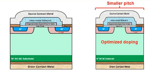
The first commercial packaged SiC MOSEFT, the CMF20120D, was introduced by Wolfspeed in January 2011 (Wolfspeed is the Power and RF division of Wolfspeed; the name was announced in 2015); SiC wafers were available a few years prior. It was rated at 1200 volts/98 A with 80 mΩ on-resistance (all at 25⁰C), and available in a TO-247 package. Wolfspeed soon followed with a 2nd generation process and is now offering 3rd generation SiC MOSEFTs designated C3M devices (Figure 2).
For example, among the members of the industry’s first 900 volt SiC MOSFET platform is the C3M0280090J. It is optimized for high frequency power electronics applications, including renewable energy inverters, electric vehicle charging systems, and three-phase industrial power supplies (Table 1).
C3M0280090J | |
|---|---|
Blocking Voltage | 900 V |
Current Rating at +25°C | 11.5 A |
RDS(ON) at +25°C | 280 Ω |
Package | TO-263-7 |
Gate Charge Total | 9.5 nC |
Maximum Junction Temperature | +150°C |
Reverse-Recovery Charge (Qrr) | 47 nC |
Reverse-Recover Time (Trr) | 20 ns |
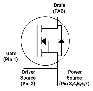
In addition to the voltage/current specifications, this device is optimized for high-speed switching with low capacitances, has a low impedance package with a driver source connection (Figure 3), includes a fast intrinsic diode with a low reverse recovery charge (Qrr), and has wide creepage (~7 millimeters (mm)) between drain and source.
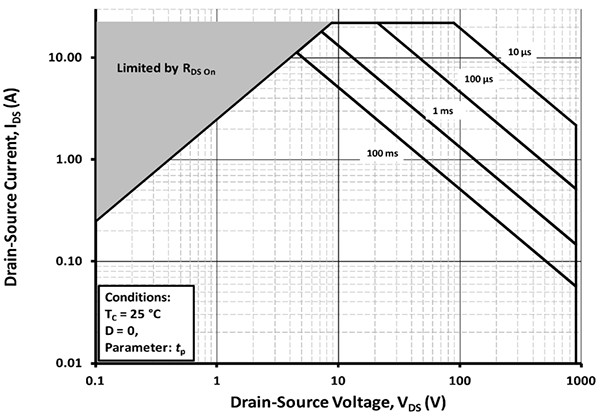
This 900 volt platform enables smaller, higher efficiency next-generation power conversion systems at a cost that is on parity with silicon-based solutions, but with superior specifications. The safe operating area (SOA) graph summarizes the capabilities of this SiC FET (Figure 4). When the drain-to-source voltage (VDS) is low, the maximum current is limited by the on-state resistance; and at moderate VDS the part can sustain 15 A for short periods of time.
Packaging affects performance
Wolfspeed also offers three devices with similar specifications—the C3M0075120D, the C3M0075120K, and the C3M0075120J—but with differences largely due to their packaging (Figure 5).
Product Name | C3M0075120D | C3M0075120K | C3M0074120J |
|---|---|---|---|
Block Voltage | 1200 V | 1200 V | 1200 V |
Current Rating at 25°C | 30 A | 30 A | 30 A |
RDS(ON) at 25°C | 75 mΩ | 75 mΩ | 75 mΩ |
Package | TO-247-3 | TO-247-4 | TO-263-7 |
Gate Charge Total | 54nC | 51nC | 51nC |
Maximum Junction Temperature | 150°C | 150°C | 150°C |
Reverse-Recovery Charge (Qrr) | -- | 220 nC | 220 nC |
Output Capacitance | 58pF | 58pF | 58pF |
Reverse-Recover Time (Trr) | 48 ns | 18 ns | 18 ns |
While the numbers provide the facts, there’s more to the story. The D suffix device is in a three-terminal package (TO-247-3), while the K suffix is in a four-terminal package (TO-247-4). These two devices, as well as the seven-terminal J suffix device, include a Kelvin source pin that reduces the effects of voltage spiking induced by L × di/dt in the gate circuit. This allows more voltage to be applied at the gate and source, resulting in faster dynamic switching. The results show a potential reduction in switching losses by a factor of 3.5 when the devices are measured near their rated current.
Evaluation boards, reference designs accelerate success
Although at the opposite end of the spectrum from gigahertz frequency RF designs, creating a high performing circuit for operation at higher voltages and power ranges still requires attention to details. Every subtlety and idiosyncrasy of the components and layout are magnified, and the physical circuit is unforgiving of the smallest issues and oversights.
To help designers evaluate SiC FETs such as the C3M0075120D and C3M0075120K, Wolfspeed offers the KIT-CRD-3DD12P buck-boost evaluation kit to demonstrate the high-speed switching performance of these devices (Figure 6). It is designed to accept both the three-terminal package of the C3M0075120D as well as the four-terminal package of the otherwise identical C3M0075120K. This enables the designer to test and compare the performance of Wolfspeed’s Generation 3 (C3M) MOSFETs in various packages.
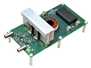
The evaluation kit comes in a half-bridge configuration and allows for the addition of a MOSFET or diode in the upper and lower positions, so the board can be configured in common power conversion topologies such as synchronous buck or synchronous boost. It also allows diodes to be added in either the top or the bottom positions, so users can evaluate an asynchronous buck or asynchronous boost converter topology.
In addition, to reduce power loss the kit comes with a low-loss inductor made up of “sendust.” Also known as Kool Mµ, this magnetic metal powder—composed of 85% iron, 9% silicon, and 6% aluminum—is used as an alternative to permalloy due to its improved specifications for key magnetic and temperature parameters.
For users who need to design their own gate driver subcircuit, Wolfspeed also offers the CGD15SG00D2 gate driver reference design for these 3rd generation SiC FETs (Figure 7).

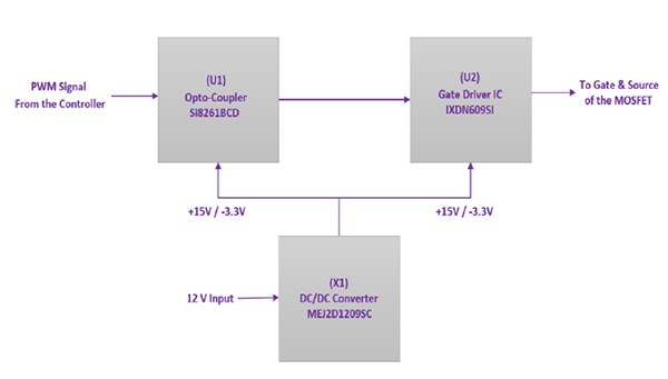
The high-level block diagram (Figure 8) of the CGD15SG00D2 shows the functions of this reference design including opto-coupler (U1), gate driver integrated circuit (U2), and isolated power supply (X1). The opto-coupler (5000 volts AC isolation) accepts pulse-width modulated (PWM) signals and provides common-mode immunity of 35/50 kilovolts (kV)/microsecond (µs) (minimum/typical). Other noteworthy features include the following:
- A groove to enhance the mandated creepage specification between the logic side and the power side of the printed circuit, and a 9 mm creepage enhancing slot between primary and secondary circuits of the board.
- A 2 watt isolated power supply that supports the operation of larger MOSFETs at higher frequencies.
- Separate gate turn-on and turn-off resistors with a dedicated diode to allow the user to customize and optimize both turn-on and turn-off signals.
- A common-mode inductor on the logic power input for enhanced EMI immunity.
Conclusion
Third generation Silicon Carbide MOSFETs from Wolfspeed offer significant performance advantages in efficiency and thermal capabilities for power switching applications compared to traditional Si MOSFETs. When combined with a suitable driver, they provide reliable, consistent performance for both emerging and established applications.