Designing with Silicon Carbide (SiC) in Electric Vehicle DC Fast Chargers
Article
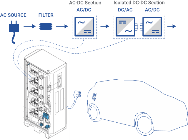
Electric Vehicle (EV) DC Fast chargers bypass the on-board charger installed on the electric vehicle and provide a fast DC charge to the battery directly. DC Fast chargers consist of an AC-DC stage and a DC-DC stage as shown below:

Minimizing charging time while optimizing system efficiency is a major focus for DC Fast chargers. Component selection, voltage range and load requirements, operating costs, temperature, ruggedness and environmental protection, and reliability must be considered when designing these systems.
SiC-based components can provide better performance than traditional Si and IGBT components due to their improved operating temperature, better conduction losses, lower leakage currents, higher surge capacity and max voltage ratings, and overall better power density. To take full advantage of these benefits, however, the power conversion topologies must be optimized.
This article will look at several power conversion topologies to consider for fast-charger systems and some tools/resources that are available, as well as a summarized table with several key comparisons.
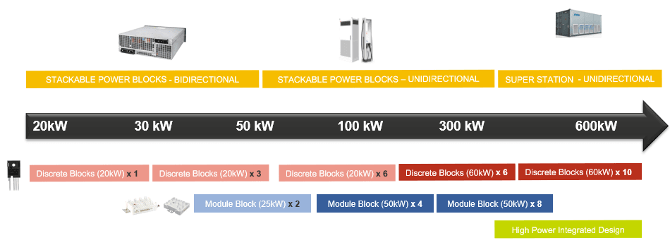
Whether in a home or public area, in a highway corridor, or for charging a fleet of vehicles, power demanded from the AC grid can range from 2.2 kW all the way to 1 MW. These systems are typically built as 20- to 50-kW AC-to-DC and DC-to-DC power blocks that can be scaled to meet higher or lower demand based on the charging location and vehicle type. A graphical view of the power levels and how systems are typically stacked is below:

The next step in the design is to analyze the practicalities in DC Fast charging applications. Firstly, these chargers are installed at public areas where a wide battery voltage and a wide load profile is expected. As an example, most EV’s on the road today have batteries in the 350-450V range while newer models are being introduced with 800V batteries. Additionally, each of these EV batteries have different charging profiles which means that EV chargers need to be designed for a wide load profile with high full load capability. Additionally, customer behavior is also important to analyze because unlike home chargers, the vehicle is almost always driven to a charging location which translates to a warm battery and a quick ramp to peak charging power. You can see this on the top left graph along with the ramp down at 80% of battery capacity as recommended by several battery manufacturers.
From a commercial operator perspective, operating costs are critical for investment. As an example, for a single 360kW charging station, 2% better efficiency for a station operating for 12 hrs/day with a 25c/kwH assumption gives a ~$22/day saving per station. The dynamic nature of the EV market also drives the need for high flexibility for new models and smaller installation footprints
Below we can summarize the system objectives for a fast charger system:
- Wide battery voltage range (350V-800V)
- Wide load profile (single/multiple vehicles) and battery buffers (for high performance vehicles)
- Optimized for charging at full load
- Bi-directionality for return-to-grid applications
- Flexible, can adapt to new industry trends/standards
- Small installation footprint
- Reduced operating costs, allow for profitability
- Rugged, wide operating temperature
Let’s explore some power topologies while keeping in mind the above requirements and design goals.
AC-DC Conversion
Topology 1 – (AC-DC): 3-Phase 2-Level Bidirectional Active Front End AC/DC Converter
The first AC/DC option is a simple six-switch, two-level active front end (AFE) configuration incorporating six Wolfspeed 1200V SiC MOSFETs (shown in Figure 1) that provides 25kW. Overall, many improvements can be observed when comparing the SiC components with IGBT devices (also shown in Figure 1).

Metric | IGBT | SiC |
|---|---|---|
Fsw | 20kHz | 45kHz |
Power Density | 3.5kW/L | 4.5kW/L |
Efficiency | 97.2% | 98.2% |
Cost | IGBT | SiC |
|---|---|---|
Switch | 32% | 62% |
Choke | 40% | 19% |
Driver | 9% | 9% |
Thermal | 19% | 10% |
Figure 1: Three-phase, two-level bidirectional AFE (top) and IGBT vs. SiC comparison (bottom)
Table 1 describes the benefits and challenges associated with this configuration.
Benefits | Challenges |
|---|---|
SiC enables smaller choke with 2.5x Fsw | Can’t reduce frequency further to balance core loss |
Low component count and low cost | High DC+/- swing adds MOSFET stress and loss |
Mature control scheme | Hard-switched topology introduces EMI concerns |
Overall simplicity | Large inherent footprint driven by size of choke |
Table 1. 3-Phase 2-Level AFE Benefits vs. Challenges
Employing six SiC MOSFETs, such as the 32-mΩ C3M0032120K by Wolfspeed, can reach a high efficiency (and reduce cost while increasing power density). Another non-discrete option is a single CCB021M12FM3 Wolfpack module providing 25kW. Using an additional module in parallel will double the power rating to 50 kW.
Design resources:
Reference design CRD22AD12N demonstrates a system with either one-phase or three-phase (grid supply) input with a non-isolated output of 650–800 VDC at 22 kW, operating at a peak efficiency of more than 98.5%.
Reference design CRD25AD12N-FMC with an AC/DC configuration consists of an active rectifier operating with three-phase input and 800-VDC output. This arrangement makes use of the CCB021M12FM3 WolfPACK™ module and can provide up to 25 kW of power with peak efficiency greater than 97%, while also providing scalability up to higher power levels by interleaving multiple 25kW AFEs.
Topology 2 – (AC-DC): T-Type Bidirectional AC/DC Converter
The T-type AC/DC converter utilizing 1,200-V SiC MOSFETs allows for lower switching losses when compared with the six-switch approach, although conduction losses dominate at full load in fast-charging applications.
Figure 4 shows a bidirectional configuration utilizing six 1,200-V 32-mΩ SiC MOSFETs used on the outer parts and another six 650-V 45-mΩ SiC MOSFETs used in the mid-section (which provides a better RDS(on) versus temperature conduction and good full-load capability). Using SiC in the mid position is also beneficial for fast-charging applications since the flat RDS(on) vs. Tj curve of silicon carbide which allows more efficient conduction at full load across operating temperatures.
Table 4 lists additional benefits and challenges associated with this implementation.
Benefits | Challenges |
|---|---|
Lower switching loss vs. six-switch | High part count |
Lower dv/dt for EMI | High component cost |
Middle 650V SiC better RDSon vs. Temp | Complex control |
Small magnetics (compared to six-switch) | Conduction loss dominates at full load in fast charger app |
Low DC+/- swing, low MOSFET stress |
Table 4. T-Type AC/DC Converter Benefits and Challenges
Topology 3 – (AC-DC): NPC/ANPC Bidirectional AC/DC Converter
Finally, a neutral-point–clamped (NPC) or active NPC topology provides a very easy transition from traditional Si to SiC. In this design, lower-voltage MOSFETs can be used alongside Schottky diodes, lowering the stress seen on the MOSFETs and switching losses (when compared with the two-level approach, as described in the previous topologies).
Figure 5 demonstrates an example of an NPC configuration and can feature 12 650-V, 25-mΩ SiC MOSFETs with six 650-V, 16-A SiC Shottky barrier diodes. The high part count, cost, and complexity are the tradeoffs for this topology.
Table 5 lists additional benefits and challenges associated with this implementation.
Benefits | Challenges |
|---|---|
650V SiC MOSFET blocks half of DC bus | High part count |
Low voltage stress | High cost |
650V SiC Diode eliminates Qrr | High complexity |
Half output transient/ripple | |
Low switching losses |
Table 5. NPC/ANPC AC/DC Converter Benefits and Challenges
Component Selection for AC-DC Topologies
For an AC/DC converter application, some decisions must be made when identifying key components in the design. To reduce crosstalk and maximize efficiency, the designer should select the highest ratio of Cgs/Cgd while using negative gate drive voltages for turn-off. And a design for full load and high power or continuous power operation should have components that favor low conduction losses. When designing for hard-switched, high-current, and high-frequency operations, choose component packages with low inductance and Kelvin pin connections like Wolfspeed K and J package styles. Additionally, selecting the lowest Qrr can provide faster recovery times and lower losses.
Table 6 shows a component count comparison for these AC/DC topologies.
AC/DC Topology | 2-level AFE (1) | T-Type (2) | NPC/ANPC (3) |
|---|---|---|---|
SiC MOSFET Count | 6 | 12 | 12 |
SiC Diode Count | 0 | 0 | 6 |
Table 6. Summary of AC/DC Fast Charger Topologies
DC-DC Conversion
Topology 1 – (DC-DC): 20-30kW 2-Level LLC Bidirectional DC/DC Converter
Figure 6 shows an example of a 2-level LLC circuit with bidirectional flow and 12 total SiC MOSFETs that enable simple, flexible control with high efficiency and small magnetics. In this configuration meant for DC fast charging, the relays can be switched in and out for 400V and 800V operation for low or high charge currents. One drawback is that LLC designs in general have a narrow sweet spot which requires careful tank design.

Table 7 lists additional benefits and challenges associated with this implementation.
Benefits | Challenges |
|---|---|
1200V SiC enables simple 2-level control | Narrow sweet spot |
Split 650V for flexible design optimized for 400V/800V outputs | |
SiC enables high switching frequency with smaller magnetics | |
Good current sharing with LLC tanks | |
High efficiency at resonance |
Table 7. 2-Level LLC DC/DC Converter Benefits and Challenges
Topology 2 – (DC-DC): 20-30kW 2-Level LLC Cascade Bidirectional DC/DC Converter
Figure 7 shows an example of a 2-level LLC cascade circuit with bidirectional flow and 12 total MOSFETs that allow for an easy transition over from traditional Si components to SiC (at 650V). Though the efficiency can be high due to the SiC components, there are several challenges (see Table 8).

Benefits | Challenges |
|---|---|
Allows for simple transition from 650V Si to 650V SiC | 2X parts count and cost |
High efficiency at resonance | Poor current sharing due to parallel resonant tanks |
Lower overall efficiency | |
Narrow sweet spot |
Table 8. 2-Level LLC Cascade DC/DC Converter Benefits and Challenges
CRD-22DD12N is a 22kW reference design from Wolfspeed that provides a great starting point for 2-level LLC DC/DC converter designs utilizing 1200V SiC MOSFETs. The design can enable 22kW of power for battery voltages up to 800V and flexibility of bidirectional power transfer, while also allowing for flexible full bridge and half-bridge schemes to adjust gain and efficiency.
One thing to consider for LLC converter designs in general is the selection of a suitable SiC MOSFET. Here are some guidelines for selecting the right MOSFET for an LLC topology.
- The MOSFET output capacitance (and time required to charge) can greatly determine the performance of converters with zero voltage switching, as seen in LLC circuits. Selecting a SiC MOSFET with the lowest value of COSS at a low VDS is best.
- The turn-off switching losses in LLC converters are proportional to the magnetizing current which is usually small for LLC designs, resulting in well controlled switching losses at turn-off.
- Since the turn-off in an LLC is hard-switched, it’s best to select a package with a Kelvin pin like the TO-247-4 or TO-263-7 packages that can reduce switching losses by up to 4X compared to 3-lead packages. Additionally, reverse recovery losses can be significant for high frequency applications, so it’s best to select components with the lowest reverse recovery times.
Topology 3 – (DC-DC): 20-30kW Dual Active Bridge (DAB) Bidirectional DC/DC Converter
Figure 8 shows an example of a 20-30kW Dual Active Bridge (phase shifted) DC/DC converter which provides a fast-charging solution with a trapezoidal current profile (as compared to the sinusoidal profiles as seen in LLC circuits). The benefits and challenges for this topology can be seen in Table 9.

Benefits | Challenges |
|---|---|
Wide output range (vs. LLC) | Lower efficiency (vs. LLC), higher turn-off current results in higher switching loss |
Simple control for charger module synchronization | Sharp current transitions may require EMI mitigation |
Narrow range of ZVS |
Table 9. DAB DC/DC Converter Benefits and Challenges
Topology 4 – (DC-DC): 30-60kW 3-Phase LLC Unidirectional DC/DC Converter
When designing DC/DC converters in the 30-60kW range, there are some additional challenges to consider, such as high ripple currents on the DC-link and output capacitors, high output filter volume (for LLC circuits), and high current levels on the primary side MOSFETs. To demonstrate solutions for these issues at 30kW, Wolfspeed created a reference design CRD-30DD12N-K. using an interleaved 3-Phase LLC topology. 60kW systems may also be designed with discrete devices although additional considerations like symmetric design with regards to current sharing and parasitic effects will need to be considered.
Designing with power modules help simplify some of these challenges by enabling matched inductances, simplified thermal designs, scalable solutions at various power levels, and allow extension of existing full-bridge topologies to much higher power levels
Figure 9 shows the interleaved 3-phase LLC DC/DC converter topology used in CRD-30DD12N-K while Table 10 describes the relative benefits and challenges.
Benefits | Challenges |
|---|---|
Low input current ripple | Tolerance of resonant capacitance/inductance and magnetizing Lm can result in unbalanced currents |
Low output ripple and smaller output capacitor | Complex vector control (3-phase analysis applies) |
Uniform distribution of power to 3-phase on primary | |
Flexible discrete solution with 1x or 2x SiC MOSFETs per position | |
Scalable to lower phases or higher number of phases |
Table 10. 3-Phase LLC DC/DC Converter Benefits and Challenges
Figure 10 and Table 11 show an alternative 50-60kW 2-level LLC resonant converter configuration that uses half-bridge Wolfspeed WolfPACK power modules in the primary and 30A Schottky diodes in the secondary.
Figure 10. 50-60kW 2-Level LLC Resonant Converter
Benefits | Challenges |
|---|---|
WolfPACK offers simple high power density primary | Tolerance of resonant capacitance/inductance and magnetizing Lm can result in unbalanced currents |
Simple control | Optimization of magnetics can result in significant design tasks |
Table 11. 2-Level LLC Resonant Converter Benefits and Challenges
Table 12 and Table 13 show a component count comparison for these DC/DC topologies.
DC/DC Topology | 2-level LLC (1) | 2-level LLC Cascade (2) | Dual Active Bridge (3) |
|---|---|---|---|
SiC MOSFET Count | 10 | 12 | 8 |
SiC Diode Count | 0 | 0 | 0 |
Table 12. Summary of DC/DC 20-30kW Fast Charger Topologies
DC/DC Topology | 3-Phase LLC (1) | LLC Resonant Converter (2) |
|---|---|---|
SiC MOSFET Count | 6 | 4 |
SiC Diode Count | 24 | 8 |
Table 13. Summary of DC/DC 50kW+ Fast Charger Topologies
Summary
To conclude, there are a variety of converter topologies for fast-charging designs that can achieve modularity, bidirectionality, full-load operation efficiency, and high-power density. SiC technology is at the heart of these fast-charger designs and converter topologies, allowing for the best performance while ensuring a long-lasting, reliable system. Most of the topologies described in this note can be easily simulated using the Wolfspeed SpeedFit 2.0 Design Simulator™.