Skip to Main Content
Contact
  • English
  • 简体中文
  • 繁體中文
View Cart
Industrial

Silicon Carbide for Energy Storage Systems

Paul Kierstead
Oct 21, 2021
  • English
  • 简体中文
  • 繁體中文
  • Share on Facebook
  • Share on Twitter
  • Share on LinkedIn
  • Share in an email

Article

It is widely realized that Silicon Carbide (SiC) is now an established technology that is transforming the power industry in many applications across the industrial, energy, and automotive segments, ranging from watts up to megawatts.

This is mainly due to its many advantages over previous implementations of silicon (Si) and insulated-gate bipolar transistors (IGBTs), including higher switching frequencies, lower operating temperatures, higher current and voltage capacities, and lower losses, which lead to increased power density, reliability, and efficiency. And because of the cooler temperatures and smaller magnetics, thermal management and power components are now becoming smaller, lighter, and cheaper, thereby lowering total BOM costs while also enabling smaller footprints.

SiC has become a mature technology and a very common solution for systems requiring power delivery, particularly charging and discharging in energy storage applications like electric-vehicle charging and solar systems with batteries. These kinds of systems usually contain several opportunities for SiC technology, such as DC/DC boost converters, bidirectional inverters (with both AC and DC elements), and flexible battery-charging circuitry. In a nutshell, SiC enables up to 3% higher system efficiency, 50% higher power density, and a reduction in passive component volume and costs.

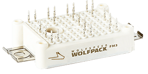
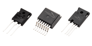
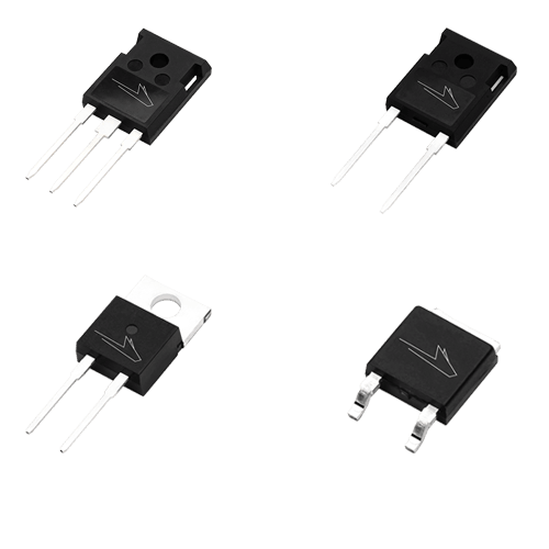
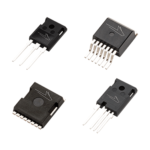
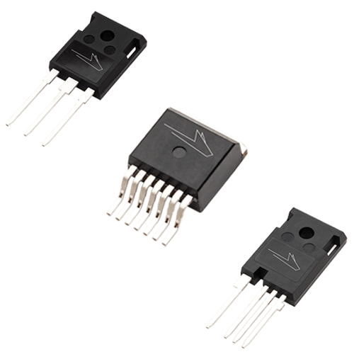
Most energy storage systems (ESS) have multiple power stages that can benefit from SiC components. Wolfspeed offers these components in several formats, such as Schottky diodes/MOSFETs (with up to 100-A current-rated packaging/196-A bare-die packaging) and power modules as seen in the WolfPACK family of devices that have up to 450-A current rating. Whether it’s a single-phase residential system (5–15 kW) or three-phase commercial system (30–100 kW), the architecture and power circuit topologies will be similar; however, they can be scaled depending on the power level.

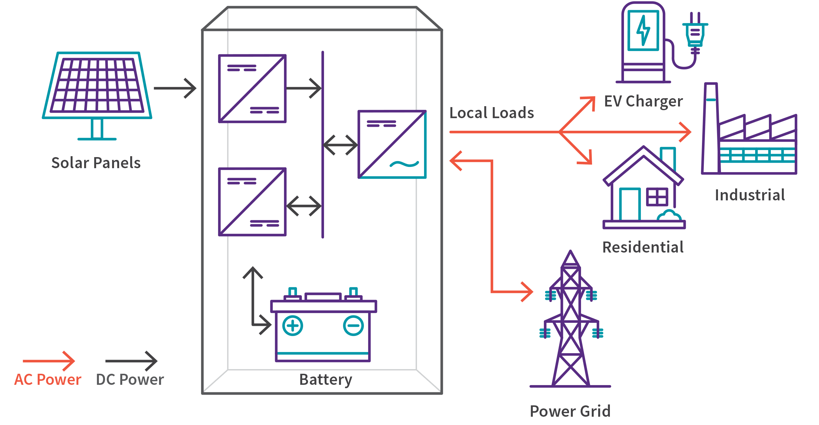
Figure 1 demonstrates a typical ESS architecture with a power source (photovoltaic, or PV, for this application, which, it is worth noting, can be replaced with any alternative energy source), a DC/DC converter, a battery charger, and an inverter for delivering energy to the home or back to the grid. In all three power blocks for this configuration, SiC can improve efficiency, size, weight, and cost.

Figure 1: ESS configuration for residential or commercial

SiC advantages in ESS power blocks

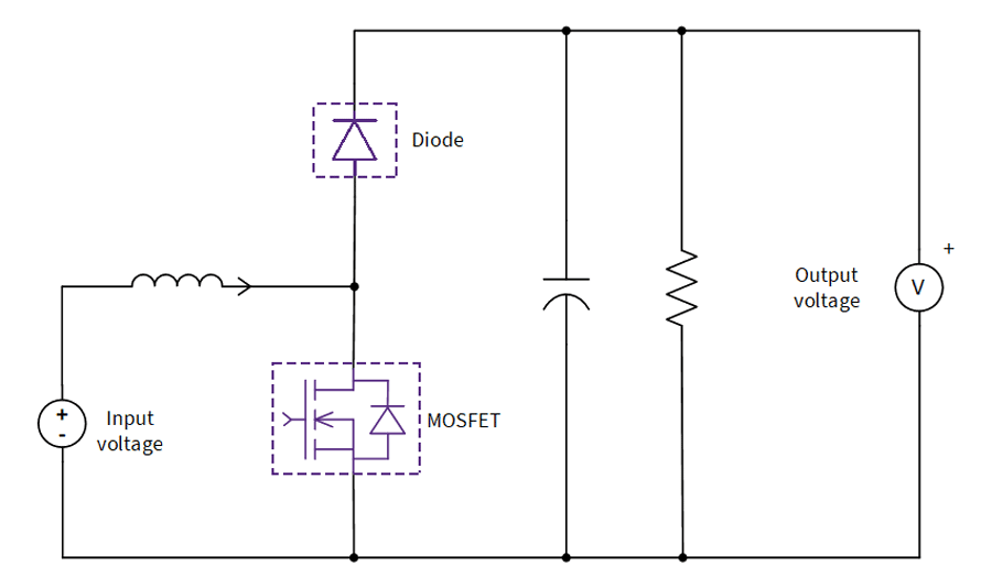
As shown above, there are several power stages involved when managing harvested energy and using it to store for later or power a home/building. The DC/DC conversion section, which often consists of a boost converter for PV applications, benefits greatly in terms of higher system efficiencies and power densities. When compared with traditional technologies such as Si, typical advantages seen with SiC include 70% reduction in system size, 60%+ reduction in energy losses, and up to 30% lower system cost.

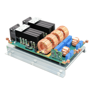
Figure 2 shows an example of a 60-kW SiC-based interleaved boost converter (from the Wolfspeed reference design CRD-60DD12N) containing several SiC MOSFETs and diodes. The four interleaved channels help scale output power up to 60 kW while keeping efficiency at 99.5% with 850 VDC on the output. This design contains two C3M0075120K MOSFETs (in a TO-247-4L package with Kelvin source pin), two C4D10120D diodes per channel, and a CGD15SGOOD2 isolated discrete gate driver.

Figure 2: 60-kW SiC-based interleaved boost converter reference design

In the reference design pictured above, a BOM cost analysis/comparison was performed at different switching frequencies. At higher frequencies (100 kHz versus 60 kHz), significant cost savings could be realized due to the smaller, lighter-weight components/magnetics, while cooling may drive up some cost due to higher operating temperatures. But overall, higher frequencies generally mean higher power density, higher system efficiency, and lower cost. This is how SiC is able to provide better performance at a lower price point.

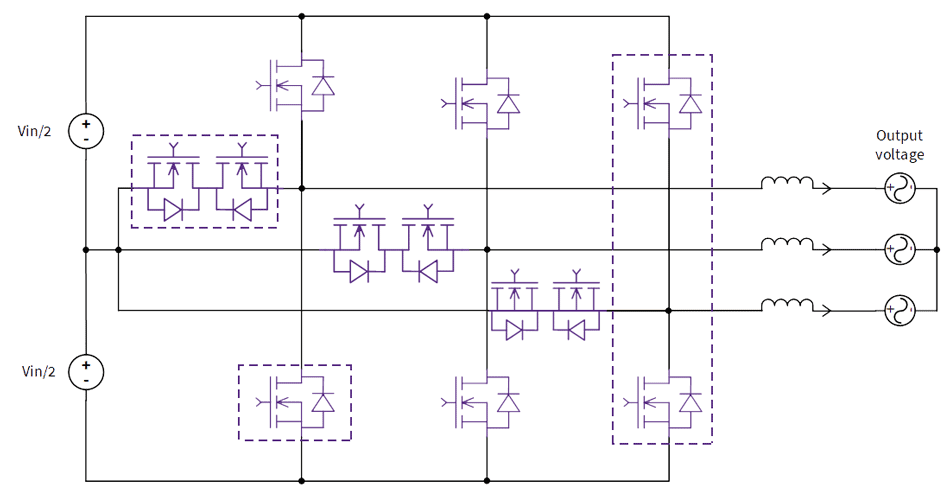
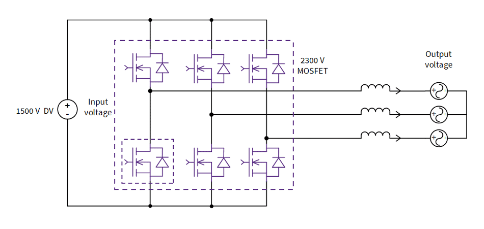
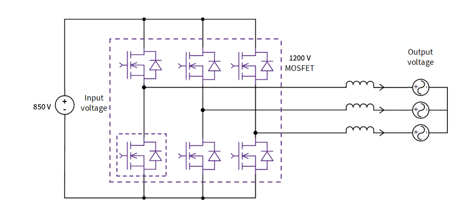
Another Wolfspeed reference design (Figure 3) highlights SiC advantages for both the inverter and DC/DC charging circuitry. This design operates in single- or three-phase mode, both charging and discharging at peak efficiencies of greater than 98.5%. The converter section consists of a simple, two-level AC/DC converter compatible with both single- and three-phase connections with only six SiC MOSFETs. This configuration isn’t as low-cost as most IGBT converters but will outperform in terms of efficiency and loss. Though the T-type AC/DC converter offers even similar switching frequency and similar efficiencies, it often involves complex control and higher part counts with a lower power density.

Figure 3: Simple two-level inverter/active front end (AFE) with SIC MOSFETs

For the design pictured above, the DC-link voltage can be up to 900 V, while battery voltage typically sits at about 800 V. Because of the electrical and thermal stress, the C3M0032120K 1200V 32-mΩ SiC MOSFET from Wolfspeed is well-suited based on its figure of merit, easy control and Vgs drive characteristics, and Kelvin source package, which reduces switching losses and reduces crosstalk.

This topology allows for advanced digital control schemes that fulfill different functions, such as a single-phase interleaved PFC scheme or a three-phase DQ transformation space-vector PWM scheme that balances switching losses in all devices making for a very flexible reference platform. Utilizing PWM control per switch can be helpful to sense and balance power dissipation while optimizing thermal performance, efficiency, and reliability.

When testing and measuring efficiency across a variety of loads and voltage ranges for single-phase charging, it was found that SiC achieves up to 98.5% efficiency, while IGBTs might top out at 96%, resulting in about 38% lower losses for SiC. Figure 4 shows two plots of the AFE for charging and discharging across a wide range of power levels.

Figure 4: AFE efficiency for charging (left) and discharging (right) modes across many power levels

For three-phase charging, the same peak efficiencies were achieved along with thermal performance operating well within the system and device limitations. Although T-type topologies can hit similar performance, it’s generally more complex and costly.

To summarize the 22-kW inverter/AFE configuration, the C3M0032120K SiC MOSFETs and the flexible control scheme enable high efficiency (>98.5%), high power density (4.6 W/L), lower loss (60%), and bidirectional chargers that can support the DC-link from both three-phase and single-phase AC inputs while outputting a wide battery voltage range of 200–800 VDC.

SiC advantages in DC/DC battery charger circuits

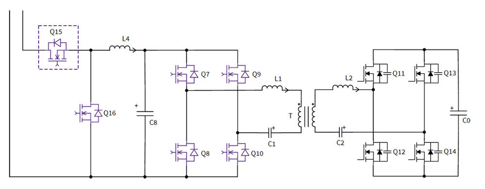
Many topologies support isolated DC/DC converters; however, the most mainstream solutions are half-bridge and full-bridge LLC converters. A reference design (CRD-22DD12N by Wolfspeed) demonstrates a 22-kW solution that can be configured for either a cascade converter or a single two-level converter. The cascade converter can either utilize 650-V Si MOSFETs or SiC components but will generally have a higher part count, higher conduction losses, higher control complexity, and higher system cost. The single two-level converter uses SiC components for the higher voltage (1,200 V) and switches at a much higher frequency of 200 kHz. The biggest SiC-based advantage here is higher efficiency/lower losses with some additional features, such as zero-voltage turn-on, low-current turn-off, and lower risk for EMI. The topology has a lower part count than the cascade converter, which helps to lower system cost and provide simpler control. Figure 5 demonstrates the differences of these two layouts.

Figure 5: 22-kW full-bridge CLLC DC/DC converter — cascade (left) and single two-level (right)

When considering power components for this 22kW design, it was again found that the C3M0032120K 1,200-V 32-mΩ MOSFET provides the best electrical stress and thermal characteristics to suit the converter. In addition, its Vgs can support 15 V, making for easy driving. A variable DC-link voltage control (based on sensed battery voltage) enables the best system efficiency and ensures that the CLLC runs close to resonant frequency. When the battery voltage is low, the control switches to phase-shift mode, which reduces gain without running inefficiently outside of the resonant frequency range. This means that with the same hardware, a similar high efficiency can be achieved at lower output voltages. And if lower battery voltage is needed, the CLLC primary can be run as a half-bridge, which further reduces gain but maintains the efficiency zone. This lower efficiency can still be acceptable due to the lower operating cost and less stringent thermal design.

Figure 6 shows waveforms for both charging and discharging modes for a full-bridge configuration. The charging mode screenshot shows zero-voltage turn-on with low-current turn-off conditions, resulting in high-efficiency operation. The waveforms are also very clean and contain low overshoot switching, which helps with EMI concerns.

Figure 6: Charging and discharging modes for 22-kW SiC DC/DC converter

The converter’s efficiency results are similar to the inverter reference design, with 98.5% peak efficiency across most of the load. The variable DC-link voltages and resultant efficiency stays above 97% until the design enters half-bridge mode, which limits efficiency and power delivery capabilities during charging. In general, the SiC MOSFETs along with the flexible control scheme enables high-efficiency (>98.5% efficiency for charging/discharging) and high-power–density (8 kW/L) bidirectional chargers that support both single-phase and three-phase AC inputs. And when compared with Si, higher efficiency and power density is achieved for significantly less cost due to the gate driver simplicity, thermal management components, reduced part counts, and smaller magnetics.

Summarizing the Wolfspeed SiC advantage

Today’s industry has greatly benefited from SiC components, primarily due to thermal properties and faster switching with lower loss. With less temperature dependence of the turn-on resistance, the MOSFET sees lower conduction loss at higher temperatures and enables high-frequency switching. In addition, the high-performance body diode allows for high reliability in resonant converter applications, while a smaller output capacitance makes it easy to achieve zero-voltage switching for LLC converters.

Figure 7 shows a direct comparison of SiC’s typical size/weight benefits over Si components (rated for 650 V). Usually, silicon components require a transformer plus the resonant inductor, while SiC configurations can get away with an integrated transformer/inductor, saving on weight and space.

Silicon Solution
SiC Solution
SiC Advantage
fs = 150kHz
fs = 500kHz
233% Faster
Transformer/inductor volume = 48 cm3
Transformer/inductor volume = 25 cm3
40% Smaller
Weight = 416g
Weight = 200g
52% Lighter

Figure 7: sic vs. Si comparison on size and weight

And in terms of efficiency, peak values can be seen at 98.5% (as shown in the examples described previously) for medium loads but greater than 97.5% at maximum loads across the entire input range. Wolfspeed’s family of SiC devices span the complete power spectrum of applications, from 1 kW up to the megawatt range with scaled, high-power modules. With discrete solutions on the low end, WolfPACK modules for mid-power levels, and high-power module solutions on the high end, the designer is provided many options for topology and sourcing while optimizing BOM costs and physical size/layout. The power modules maximize power density, simplify layout and assembly (with industry-standard footprints), enable scalability for higher-power systems, and maintain the highest efficiency and reliability with lower labor and component costs.

Reference designs and evaluation kits are provided for several topologies, such as AC/DC power-factor correction, buck/boost DC/DC, high-frequency DC/DC, and bidirectional AC/DC, DC/DC, and DC/AC kits. The SpeedFit design simulator helps to characterize system-level circuits, model common topologies, and select the right SiC device for your application.

Whether using discretes or high-power modules, SiC has shown tremendous opportunity in energy storage applications from residential through industrial, and Wolfspeed’s portfolio/resources enable the most flexible, scalable, high-performance designs at a low cost and small footprint.

Watch the Webinar

Technical SupportPower Applications Forum

More Articles

View All
Power
|
Industrial Drives

Benefits of Designing with Wolfspeed Silicon Carbide in Low Voltage Motor Drives

Continue Reading  Technical Articles

Footer

Social Media

  • Facebook
  • Instagram
  • X
  • LinkedIn
  • YouTube
Copyright © 2024 Wolfspeed, Inc.